CHAPTER 1
Sarah L. Harris and David Money Harris, Digital Design and Computer Architecture: ARM® Edition © 2015 by Elsevier Inc.
Exercise Solutions
SOLUTIONS

SOLUTIONS 1
Sarah L. Harris and David Money Harris, Digital Design and Computer Architecture: ARM® Edition © 2015 by Elsevier Inc.
Exercise Solutions
CHAPTER 1
Exercise 1.1
(a) Biologists study cells at many levels. The cells are built from organelles
such as the mitochondria, ribosomes, and chloroplasts. Organelles are built of
macromolecules such as proteins, lipids, nucleic acids, and carbohydrates.
These biochemical macromolecules are built simpler molecules such as carbon
chains and amino acids. When studying at one of these levels of abstraction, bi-
ologists are usually interested in the levels above and below: what the structures
at that level are used to build, and how the structures themselves are built.
(b) The fundamental building blocks of chemistry are electrons, protons,
and neutrons (physicists are interested in how the protons and neutrons are
built). These blocks combine to form atoms. Atoms combine to form molecules.
For example, when chemists study molecules, they can abstract away the lower
levels of detail so that they can describe the general properties of a molecule
such as benzene without having to calculate the motion of the individual elec-
trons in the molecule.
Exercise 1.3
Ben can use a hierarchy to design the house. First, he can decide how many
bedrooms, bathrooms, kitchens, and other rooms he would like. He can then
jump up a level of hierarchy to decide the overall layout and dimensions of the
house. At the top-level of the hierarchy, he material he would like to use, what
kind of roof, etc. He can then jump to an even lower level of hierarchy to decide
the specific layout of each room, where he would like to place the doors, win-
dows, etc. He can use the principle of regularity in planning the framing of the
house. By using the same type of material, he can scale the framing depending
on the dimensions of each room. He can also use regularity to choose the same
(or a small set of) doors and windows for each room. That way, when he places

2 SOLUTIONS chapter 1
Sarah L. Harris and David Money Harris, Digital Design and Computer Architecture: ARM® Edition © 2015
by Elsevier Inc. Exercise Solutions
a new door or window he need not redesign the size, material, layout specifica-
tions from scratch. This is also an example of modularity: once he has designed
the specifications for the windows in one room, for example, he need not re-
specify them when he uses the same windows in another room. This will save
him both design time and, thus, money. He could also save by buying some
items (like windows) in bulk.
Exercise 1.5
(a) The hour hand can be resolved to 12 * 4 = 48 positions, which represents
log
2
48 = 5.58 bits of information. (b) Knowing whether it is before or after noon
adds one more bit.
Exercise 1.7
2
16
= 65,536 numbers.
Exercise 1.9
(a) 2
16
-1 = 65535; (b) 2
15
-1 = 32767; (c) 2
15
-1 = 32767
Exercise 1.11
(a) 0; (b) -2
15
= -32768; (c) -(2
15
-1) = -32767
Exercise 1.13
(a) 10; (b) 54; (c) 240; (d) 2215
Exercise 1.15
(a) A; (b) 36; (c) F0; (d) 8A7
Exercise 1.17
(a) 165; (b) 59; (c) 65535; (d) 3489660928
Exercise 1.19
(a) 10100101; (b) 00111011; (c) 1111111111111111;
(d) 11010000000000000000000000000000

SOLUTIONS 3
Sarah L. Harris and David Money Harris, Digital Design and Computer Architecture: ARM® Edition © 2015 by Elsevier
Inc. Exercise Solutions
Exercise 1.21
(a) -6; (b) -10; (c) 112; (d) -97
Exercise 1.23
(a) -2; (b) -22; (c) 112; (d) -31
Exercise 1.25
(a) 101010; (b) 111111; (c) 11100101; (d) 1101001101
Exercise 1.27
(a) 2A; (b) 3F; (c) E5; (d) 34D
Exercise 1.29
(a) 00101010; (b) 11000001; (c) 01111100; (d) 10000000; (e) overflow
Exercise 1.31
00101010; (b) 10111111; (c) 01111100; (d) overflow; (e) overflow
Exercise 1.33
(a) 00000101; (b) 11111010
Exercise 1.35
(a) 00000101; (b) 00001010
Exercise 1.37
(a) 52; (b) 77; (c) 345; (d) 1515
Exercise 1.39
(a) 100010
2
, 22
16
, 34
10
; (b) 110011
2
, 33
16
, 51
10
; (c) 010101101
2
, AD
16
,
173
10
; (d) 011000100111
2
, 627
16
, 1575
10
Exercise 1.41
15 greater than 0, 16 less than 0; 15 greater and 15 less for sign/magnitude

4 SOLUTIONS chapter 1
Sarah L. Harris and David Money Harris, Digital Design and Computer Architecture: ARM® Edition © 2015
by
Elsevier Inc. Exercise Solutions
Exercise 1.43
4, 8
Exercise 1.45
5,760,000
EExercise 1.47
46.566 gigabytes
Exercise 1.49
128 kbits
Exercise 1.51
Exercise 1.53
(a) 11011101; (b) 110001000 (overflows)
Exercise 1.55
(a) 11011101; (b) 110001000
Exercise 1.57
(a) 000111 + 001101 = 010100
(b) 010001 + 011001 = 101010, overflow
(c) 100110 + 001000 = 101110
-2 -1 0 1 2 3
10 11 00 01
Two's Complement
10
11
00
01
00 01 10 11
Sign/Magnitude
Unsigned

SOLUTIONS 5
Sarah L. Harris and David Money Harris, Digital Design and Computer Architecture: ARM® Edition © 2015 by Elsevier
Inc. Exercise Solutions
(d) 011111 + 110010 = 010001
(e) 101101 + 101010 = 010111, overflow
(f) 111110 + 100011 = 100001
Exercise 1.59
(a) 0x2A; (b) 0x9F; (c) 0xFE; (d) 0x66, overflow
Exercise 1.61
(a) 010010 + 110100 = 000110; (b) 011110 + 110111 = 010101; (c) 100100
+ 111101 = 100001; (d) 110000 + 101011 = 011011, overflow
Exercise 1.63
Exercise 1.65
(a) 0011 0111 0001
(b) 187
(c) 95 = 1011111
(d) Addition of BCD numbers doesn't work directly. Also, the representa-
tion doesn't maximize the amount of information that can be stored; for example
2 BCD digits requires 8 bits and can store up to 100 values (0-99) - unsigned 8-
bit binary can store 28 (256) values.
Exercise 1.67
Both of them are full of it. 42
10
= 101010
2
, which has 3 1’s in its represen-
tation.
Exercise 1.69
#include <stdio.h>
void main(void)
{
char bin[80];
int i = 0, dec = 0;
printf("Enter binary number: ");
scanf("%s", bin);
-3-2-101234
000 001 010 011 100 101 110 111
Biased

6 SOLUTIONS chapter 1
Sarah L. Harris and David Money Harris, Digital Design and Computer Architecture: ARM® Edition © 2015
by
Elsevier Inc. Exercise Solutions
while (bin[i] != 0) {
if (bin[i] == '0') dec = dec * 2;
else if (bin[i] == '1') dec = dec * 2 + 1;
else printf("Bad character %c in the number.\n", bin[i]);
i = i + 1;
}
printf("The decimal equivalent is %d\n", dec);
}
Exercise 1.71
Exercise 1.73
Exercise 1.75
XOR3
Y = A + B + C
BCY
00
01
10
11
A
BY
C
A
0
0
0
0
00
01
10
11
1
1
1
1
0
1
1
0
1
0
0
1
XNOR4
Y = A + B + C + D
A
B
Y
C
BDY
001
010
100
111
C
0
0
0
0
000
011
101
110
1
1
1
1
A
000
011
101
110
0
0
0
0
001
010
100
111
1
1
1
1
0
0
0
0
0
0
0
0
1
1
1
1
1
1
1
1
D
OR3
Y = A+B+C
BCY
00
01
10
11
A
BY
C
A
0
0
0
0
00
01
10
11
1
1
1
1
0
1
1
1
1
1
1
1
(a) (b)
(c)
BCY
00
01
10
11
A
0
0
0
0
00
01
10
11
1
1
1
1
0
0
0
1
0
1
1
1

SOLUTIONS 7
Sarah L. Harris and David Money Harris, Digital Design and Computer Architecture: ARM® Edition © 2015 by Elsevier
Inc. Exercise Solutions
Exercise 1.77
Exercise 1.79
No, there is no legal set of logic levels. The slope of the transfer character-
istic never is better than -1, so the system never has any gain to compensate for
noise.
Exercise 1.81
The circuit functions as a buffer with logic levels V
IL
= 1.5; V
IH
= 1.8; V
OL
= 1.2; V
OH
= 3.0. It can receive inputs from LVCMOS and LVTTL gates be-
cause their output logic levels are compatible with this gate’s input levels. How-
ever, it cannot drive LVCMOS or LVTTL gates because the 1.2 V
OL
exceeds
the V
IL
of LVCMOS and LVTTL.
Exercise 1.83
(a) XOR gate; (b) V
IL
= 1.25; V
IH
= 2; V
OL
= 0; V
OH
= 3
Exercise 1.85
BCY
00
01
10
11
A
0
0
0
0
00
01
10
11
1
1
1
1
1
1
1
0
1
0
1
0
2
2
N

8 SOLUTIONS chapter 1
Sarah L. Harris and David Money Harris, Digital Design and Computer Architecture: ARM® Edition © 2015
by Elsevier Inc. Exercise Solutions
Exercise 1.87
XOR
Exercise 1.89
Question 1.1
A
B
C
Y
(b) (c)
Y
A
B
AB
A
B
C
Y
(a)
ABY
000
011
101
110
(a) (b) (c)
ABC
Y
A
B
C
Y
A
B
C
Y
weak
weak
weak
A
B
C
Y
D

SOLUTIONS 9
Sarah L. Harris and David Money Harris, Digital Design and Computer Architecture: ARM® Edition © 2015 by Elsevier
Inc. Exercise Solutions
Question 1.3
17 minutes: (1) designer and freshman cross (2 minutes); (2) freshman re-
turns (1 minute); (3) professor and TA cross (10 minutes); (4) designer returns
(2 minutes); (5) designer and freshman cross (2 minutes).

SOLUTIONS 11
Sarah L. Harris and David Money Harris, Digital Design and Computer Architecture: ARM® Edition © 2015 by Elsevier
Inc. Exercise Solutions
CHAPTER 2
Exercise 2.1
(a)
(b)
(c)
(d)
(e)
Exercise 2.3
(a)
(b)
(c)
(d)
(e)
Y ABABAB++=
Y ABC ABC+=
Y ABC ABC ABC ABC ABC++++=
Y ABCD ABCD ABCD ABCD ABCD ABCD ABCD++++++=
Y ABCD ABCD ABCD ABCD ABCD ABCD ABCD ABCD+++++++=
YAB+=
Y ABC++ABC++ABC++ABC++ABC++ABC++=
Y ABC++ABC++ABC++=
Y ABCD+++ABCD+++ABCD+++ABCD+++ABCD+++
ABCD+++ABCD+++ABCD+++ABCD+++
=
Y ABCD+++ABCD+++ABCD+++ABCD+++ABCD+++
ABCD+++ABCD+++ABCD+++
=

12 SOLUTIONS chapter 2
Sarah L.
Harris and David Money Harris, Digital Design and Computer Architecture: ARM® Edition © 2015
by Elsevier Inc. Exercise Solutions
Exercise 2.5
(a)
(b)
(c)
(d)
(e)
This can also be expressed as:
Exercise 2.7
(a)
(b)
(c)
YAB+=
Y ABC ABC+=
YACABAC++=
YABBDACD++=
Y ABCD ABCD ABCD ABCD ABCD ABCD ABCD ABCD+++++++=
YABCDABCD+=
A
B
Y
A
B
Y
C
A
B
Y
C

SOLUTIONS 13
Sarah L. Harris and David Money Harris, Digital Design and Computer Architecture: ARM® Edition © 2015 by Elsevier
Inc. Exercise Solutions
(d)
(e)
Exercise 2.9
(a) Same as 2.7(a)
(b)
(c)
AB
Y
C D
A
B
Y
C
D
A
B
Y
C
AB
Y
C
14 SOLUTIONS chapter 2
Sarah L.
Harris and David Money Harris, Digital Design and Computer Architecture: ARM® Edition © 2015
by Elsevier Inc. Exercise Solutions
(d)
(e)
Exercise 2.11
(a)
(b)
AB
Y
C D
Y
A B C D
A
B
Y
A
B
Y
C

SOLUTIONS 15
Sarah L. Harris and David Money Harris, Digital Design and Computer Architecture: ARM® Edition © 2015 by Elsevier
Inc. Exercise Solutions
(c)
(d)
(e)
Exercise 2.13
(a) Y = AC + BC
(b) Y = A
(c) Y = A + B C + B D + BD
Exercise 2.15
(a)
A
B
Y
C
A
B
Y
C
D
A
B
C
D
Y
A
BY
C

16 SOLUTIONS chapter 2
Sarah L.
Harris and David Money Harris, Digital Design and Computer Architecture: ARM® Edition © 2015
by Elsevier Inc. Exercise Solutions
(b)
(c)
Exercise 2.17
(a)
(b)
(c)
Exercise 2.19
AY
A
B
Y
C
D
YBAC+=
B
Y
C
A
YAB=
B
Y
A
YABCDE++=
B
Y
ADCE

SOLUTIONS 17
Sarah L. Harris and David Money Harris, Digital Design and Computer Architecture: ARM® Edition © 2015 by Elsevier
Inc. Exercise Solutions
4 gigarows = 4 x 2
30
rows = 2
32
rows, so the truth table has 32 inputs.
Exercise 2.21
Ben is correct. For example, the following function, shown as a K-map, has
two possible minimal sum-of-products expressions. Thus, although and
are both prime implicants, the minimal sum-of-products expression does
not have both of them.
Exercise 2.23
Exercise 2.25
ACD
BCD
01 11
1
0
0
0
1
1
1
001
0
1
0
0
0
0
0
0
11
10
00
00
10
AB
CD
Y
ABD
ACD
ABC
Y = ABD + ABC + ACD
01 11
1
0
0
0
1
1
1
001
0
1
0
0
0
0
0
0
11
10
00
00
10
AB
CD
Y
ABD
ABC
Y = ABD + ABC + BCD
BCD
00
01
10
11
B
2
0
0
0
0
00
01
10
11
1
1
1
1
1
1
1
1
1
1
1
0
1
1
1
1
1
1
1
0
B
1
B
0
B
2
B
1
B
0
B
2
+ B
1
+ B
0
18 SOLUTIONS chapter 2
Sarah L.
Harris and David Money Harris, Digital Design and Computer Architecture: ARM® Edition © 2015
by Elsevier Inc. Exercise Solutions
Exercise 2.27
01 11
0
1
0
1
0
1
0
101
1
0
1
0
1
0
1
1
11
10
00
00
10
AB
CD
Y
D
ABC
01 11
0
0
0
1
1
1
0
101
0
0
1
0
1
0
0
0
11
10
00
00
10
AB
CD
Z
BD
Y = ABC + D
ACD
Z = ACD + BD
D
Y
BAC
Z

SOLUTIONS 19
Sarah L. Harris and David Money Harris, Digital Design and Computer Architecture: ARM® Edition © 2015 by Elsevier
Inc. Exercise Solutions
Exercise 2.29
Two possible options are shown below:
Exercise 2.31
Exercise 2.33
The equation can be written directly from the description:
A
B
D
E
F
Y
G
C
Y = ABC + D + (F + G)E
= ABC + D + EF + EG
A
B
C
D
Y
(b)(a)
C
A
D
B
Y
Y ADABCDBDCD+++ABCDDABC+++==
ESAALH++=

20 SOLUTIONS chapter 2
Sarah L.
Harris and David Money Harris, Digital Design and Computer Architecture: ARM® Edition © 2015
by Elsevier Inc. Exercise Solutions
Exercise 2.35
P has two possible minimal solutions:
Hardware implementations are below (implementing the first minimal
equation given for P).
00
01
10
11
0
0
0
0
00
01
10
11
1
1
1
1
0
0
1
1
0
1
0
1
00
01
10
11
0
0
0
0
00
01
10
11
1
1
1
1
0
0
0
0
0
0
0
0
1
1
1
1
1
1
1
1
0
0
0
1
0
1
0
0
A
3
A
1
A
2
A
0
PD
0
0
0
1
0
0
1
0
0
1
0
0
1
0
0
1
Decimal
Value
0
1
2
3
4
5
6
7
8
9
10
11
12
13
14
15
01 11
0
0
0
0
1
0
0
101
1
0
0
1
1
0
0
0
11
10
00
00
10
A
3:2
D
A
1:0
01 11
0
0
0
1
0
1
0
001
1
1
1
0
0
0
1
0
11
10
00
00
10
A
3:2
P
A
1:0
D = A
3
A
2
A
1
A
0
+ A
3
A
2
A
1
A
0
+ A
3
A
2
A
1
A
0
+ A
3
A
2
A
1
A
0
+ A
3
A
2
A
1
A
0
P = A
3
A
2
A
0
+ A
3
A
1
A
0
+ A
3
A
2
A
1
+ A
2
A
1
A
0
P = A
3
A
1
A
0
+ A
3
A
2
A
1
+ A
2
A
1
A
0
+ A
2
A
1
A
0

SOLUTIONS 21
Sarah L. Harris and David Money Harris, Digital Design and Computer Architecture: ARM® Edition © 2015 by Elsevier
Inc. Exercise Solutions
Exercise 2.37
The equations and circuit for Y
2:0
is the same as in Exercise 2.25, repeated
here for convenience.
A
3
A
1
A
2
A
0
D
P
01
1X
XX
0
0
1
XX
XX
XX
XX
X
X
X
X
XXX
0
0
0
1
X
X
X
X
A
3
A
1
A
2
A
0
Y
2
0
0
0
0
1
1
1
1
00
00
00
0
0
0
00
01
1X
XX
0
0
0
1
XXX
0
0
0
0
0
0
0
1
A
7
A
5
A
6
A
4
Y
1
0
0
1
1
0
0
1
1
Y
0
0
1
0
1
0
1
0
1
00000000000
Y
2
A
7
A
6
A
5
A
4
+++=
Y
1
A
7
A
6
A
5
A
4
A
3
A
5
A
4
A
2
++ +=

22 SOLUTIONS chapter 2
Sarah L.
Harris and David Money Harris, Digital Design and Computer Architecture: ARM® Edition © 2015
by Elsevier Inc. Exercise Solutions
Y
0
A
7
A
6
A
5
A
6
A
4
A
3
A
6
A
4
A
2
A
1
++ +=
A
7
A
5
A
6
A
4
A
3
A
1
A
2
A
0
Y
2
Y
1
Y
0
NONE

SOLUTIONS 23
Sarah L. Harris and David Money Harris, Digital Design and Computer Architecture: ARM® Edition © 2015 by Elsevier
Inc. Exercise Solutions
The truth table, equations, and circuit for Z
2:0
are as follows.
11
01
01
0
1
0
01
01
01
01
0
0
0
0
1X
1X
1X
1X
1
0
0
0
1X0
0
0
1
0
0
0
0
0
1
0
0
0
A
3
A
1
A
2
A
0
Z
2
0
0
0
0
0
0
0
0
0
0
0
0
00
00
00
0
0
0
01
10
00
00
0
0
1
0
00
00
01
10
0
0
0
0
01
0
0
0
0
0
0
1
0
0
0
0
0
A
7
A
5
A
6
A
4
0
Z
1
0
0
0
0
0
0
0
0
0
0
0
0
Z
0
0
0
0
0
0
0
0
1
1
1
1
1
1X
XX
XX
0
1
1
XX
XX
XX
XX
1
1
1
X
XX
XX
XX
XX
X
X
X
X
XXX
0
1
0
0
0
0
1
1
1
1
X
X
0
0
0
0
0
0
0
0
0
0
1
1
00
00
01
0
0
0
10
00
00
01
0
1
0
0
10
00
00
11
0
1
0
0
01
1
0
0
0
0
1
0
0
0
1
0
01
0
1
1
1
1
1
1
1
1
0
0
1
0
0
0
0
0
1
1
1
1
0
0
1
1
1
1
1
0
0
0
1
0
1
1
0
XX
XX
XX
X
X
X
XXX
X
X
X
X
01
1X
1X
0
1
0
X1
1
0
1
1X
Z
2
A
4
A
5
A
6
A
7
++A
5
A
6
A
7
+A
6
A
7
++=
Z
1
A
2
A
3
A
4
A
5
A
6
A
7
++++
A
3
A
4
A
5
A
6
A
7
+++A
6
A
7
+
+
=
Z
0
A
1
A
2
A
3
A
4
A
5
A
6
A
7
+++++
A
3
A
4
A
5
A
6
A
7
+++A
5
A
6
A
7
+
+
+
=

24 SOLUTIONS chapter 2
Sarah L.
Harris and David Money Harris, Digital Design and Computer Architecture: ARM® Edition © 2015
by Elsevier Inc. Exercise Solutions
Exercise 2.39
Exercise 2.41
A
7
A
5
A
6
A
4
A
3
A
1
A
2
A
0
Z
2
Z
1
Z
0
YACD+ ACDCD++==
ABY
00
010
100
11
00
Y
01
10
11
AB
AY
0
1
0
1
A
Y
BC
AB Y
001
010
100
110
0
0
0
0
00
01
10
11
1
1
1
1
0
0
0
1
C
AB
(a)
000
001
010
011
100
101
110
111
C
C
C
C
BC
B
C
(b) (c)
Y

SOLUTIONS 25
Sarah L. Harris and David Money Harris, Digital Design and Computer Architecture: ARM® Edition © 2015 by Elsevier
Inc. Exercise Solutions
Exercise 2.43
t
pd
= 3t
pd_NAND2
= 60 ps
t
cd
= t
cd_NAND2
= 15 ps
Exercise 2.45
t
pd
= t
pd_NOT
+ t
pd_AND3
= 15 ps + 40 ps
= 55 ps
t
cd
= t
cd_AND3
= 30 ps
A
2
A
1
A
0
Y
7
Y
6
Y
5
Y
4
Y
3
Y
2
Y
1
Y
0

26 SOLUTIONS chapter 2
Sarah L. Harris and David Money Harris, Digital Design and Computer Architecture: ARM® Edition © 2015
by Elsevier Inc. Exercise Solutions
Exercise 2.47
t
pd
= t
pd_INV
+ 3t
pd_NAND2
+ t
pd_NAND3
= [15 + 3 (20) + 30] ps
= 105 ps
t
cd
= t
cd_NOT
+ t
cd_NAND2
= [10 + 15] ps
= 25 ps
A
7
A
5
A
6
A
4
A
3
A
1
A
2
A
0
Y
2
Y
1
Y
0
NONE

SOLUTIONS 27
Sarah L. Harris and David Money Harris, Digital Design and Computer Architecture: ARM® Edition © 2015 by Elsevier
Inc. Exercise Solutions
Question 2.1
Question 2.3
A tristate buffer has two inputs and three possible outputs: 0, 1, and Z. One
of the inputs is the data input and the other input is a control input, often called
the enable input. When the enable input is 1, the tristate buffer transfers the data
input to the output; otherwise, the output is high impedance, Z. Tristate buffers
are used when multiple sources drive a single output at different times. One and
only one tristate buffer is enabled at any given time.
Question 2.5
A circuit’s contamination delay might be less than its propagation delay be-
cause the circuit may operate over a range of temperatures and supply voltages,
for example, 3-3.6 V for LVCMOS (low voltage CMOS) chips. As temperature
increases and voltage decreases, circuit delay increases. Also, the circuit may
have different paths (critical and short paths) from the input to the output. A gate
itself may have varying delays between different inputs and the output, affect-
ing the gate’s critical and short paths. For example, for a two-input NAND gate,
a HIGH to LOW transition requires two nMOS transistor delays, whereas a
LOW to HIGH transition requires a single pMOS transistor delay.
A
B
Y

SOLUTIONS 41
Sarah L. Harris and David Money Harris, Digital Design and Computer Architecture: ARM® Edition © 2015 by Elsevier
Inc. Exercise Solutions
CHAPTER 3
Exercise 3.1
Exercise 3.3
S
R
Q
clk
D
Q

42 SOLUTIONS chapter 3
Sarah L.
Harris and David Money Harris, Digital Design and Computer Architecture: ARM® Edition © 2015
by Elsevier Inc. Exercise Solutions
Exercise 3.5
Exercise 3.7
The circuit is sequential because it involves feedback and the output de-
pends on previous values of the inputs. This is a SR latch. When S
= 0 and R =
1, the circuit sets Q to 1. When S
= 1 and R = 0, the circuit resets Q to 0. When
both S
and R are 1, the circuit remembers the old value. And when both S and R
are 0, the circuit drives both outputs to 1.
Exercise 3.9
Exercise 3.11
If A and B have the same value, C takes on that value. Otherwise, C retains
its old value.
clk
D
Q
Q
clk

SOLUTIONS 43
Sarah L. Harris and David Money Harris, Digital Design and Computer Architecture: ARM® Edition © 2015 by Elsevier
Inc. Exercise Solutions
Exercise 3.13
Exercise 3.15
Exercise 3.17
If N is even, the circuit is stable and will not oscillate.
Exercise 3.19
The system has at least five bits of state to represent the 24 floors that the
elevator might be on.
Exercise 3.21
The FSM could be factored into four independent state machines, one for
each student. Each of these machines has five states and requires 3 bits, so at
least 12 bits of state are required for the factored design.
Q
Q
R
R
D
R
clk
CLK
Q
Q
D
Set
Set
Set
Set

44 SOLUTIONS chapter 3
Sarah L. Harris and David Money Harris, Digital Design and Computer Architecture: ARM® Edition © 2015
by
Elsevier Inc. Exercise Solutions
Exercise 3.23
This finite state machine asserts the output Q when A AND B is TRUE.
state encoding
s
1:0
S0 00
S1 01
S2 10
TABLE 3.1 State encoding for Exercise 3.23
current state inputs next state output
s
1
s
0
a b s '
1
s '
0
q
000X000
0 0 1 X 0 1 0
01X0000
0 1 X 1 1 0 0
1011101
1 0 0 0 0 0 0
1001000
1 0 1 0 0 0 0
TABLE 3.2 Combined state transition and output table with binary encodings for Exercise 3.23
S'
1
S
1
S
0
BS
1
AB+=
S'
0
S
1
S
0
A=
Q' S
1
AB=

SOLUTIONS 45
Sarah L. Harris and David Money Harris, Digital Design and Computer Architecture: ARM® Edition © 2015 by Elsevier
Inc. Exercise Solutions
Exercise 3.25
state encoding
s
1:0
S0 000
S1 001
TABLE 3.3 State encoding for Exercise 3.25
S
1
S
0
S'
1
S'
0
CLK
Reset
BA
S
1
S
0
r
Q
reset
S0 S1 S2 S3
S4
0/0
1/0
0/0
1/0 0/0
1/1
1/0
1/0
0/1
0/0

46 SOLUTIONS chapter 3
Sarah L.
Harris and David Money Harris, Digital Design and Computer Architecture: ARM® Edition © 2015
by Elsevier Inc. Exercise Solutions
S2 010
S3 100
S4 101
state encoding
s
1:0
TABLE 3.3 State encoding for Exercise 3.25
current state input next state output
s
2
s
1
s
0
a s '
2
s '
1
s '
0
q
000 00000
0 0 0 1 0 0 1 0
001 00000
0 0 1 1 0 1 0 0
010 01000
0 1 0 1 1 0 1 0
100 00000
1 0 0 1 0 0 1 1
101 01001
1 0 1 1 1 0 1 0
TABLE 3.4 Combined state transition and output table with binary encodings for Exercise 3.25
S'
2
S
2
S
1
S
0
S
2
S
1
S
0
+=
S'
1
S
2
S
1
S
0
A=
S'
0
AS
2
S
0
S
2
S
1
+=
QS
2
S
1
S
0
AS
2
S
1
S
0
A+=

SOLUTIONS 47
Sarah L. Harris and David Money Harris, Digital Design and Computer Architecture: ARM® Edition © 2015 by Elsevier
Inc. Exercise Solutions
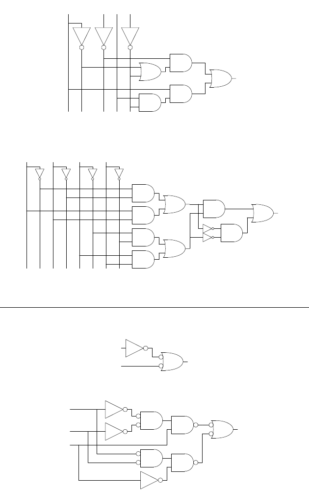
Exercise 3.27
S
2
S
1
S'
2
S'
1
CLK
Reset
A
S
1
S
0
r
S
0
S'
0
S
2

48 SOLUTIONS chapter 3
Sarah L. Harris and David Money Harris, Digital Design and Computer Architecture: ARM® Edition © 2015
by
Elsevier Inc. Exercise Solutions
FIGURE 3.1 State transition diagram for Exercise 3.27
S000
S001
S011
S010
S110
S111
S101
S100
Reset

SOLUTIONS 49
Sarah L. Harris and David Money Harris, Digital Design and Computer Architecture: ARM® Edition © 2015 by Elsevier
Inc. Exercise Solutions
current
state
s
2:0
next state
s '
2:0
000 001
001 011
011 010
010 110
110 111
111 101
101 100
100 000
TABLE 3.5 State transition table for Exercise 3.27
S'
2
S
1
S
0
S
2
S
0
+=
S'
1
S
2
S
0
S
1
S
0
+=
S'
0
S
2
S
1
=
Q
2
S
2
=
Q
1
S
1
=
Q
0
S
0
=

50 SOLUTIONS chapter 3
Sarah L.
Harris and David Money Harris, Digital Design and Computer Architecture: ARM® Edition © 2015
by Elsevier Inc. Exercise Solutions
FIGURE 3.2 Hardware for Gray code counter FSM for Exercise 3.27
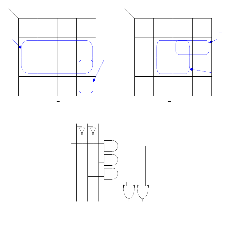
Exercise 3.29
(a)
FIGURE 3.3 Waveform showing Z output for Exercise 3.29
(b) This FSM is a Mealy FSM because the output depends on the current
value of the input as well as the current state.
S
2
S
1
S'
2
S'
1
CLK
Reset
S
1
S
0
r
S
0
S'
0
S
2
Q
2
Q
1
Q
0
CLK
A
B
Z

SOLUTIONS 51
Sarah L. Harris and David Money Harris, Digital Design and Computer Architecture: ARM® Edition © 2015 by Elsevier
Inc. Exercise Solutions
(c)
FIGURE 3.4 State transition diagram for Exercise 3.29
(Note: another viable solution would be to allow the state to transition from
S0 to S1 on . The arrow from S0 to S0 would then be .)
Reset
S0
S1
S2
BA/0
S3
BA/0BA/1BA/0
BA/1BA/1
A/0
BA/0
BA/1
BA/1
BA/1
BA/1
BA/1
BA/0
BA/0
BA 0
BA 0
current state
s
1:0
inputs next state
s '
1:0
o u t p u t
z
b a
00 X 0 00 0
00 0 1 11 0
00 1 1 01 1
01 0 0 00 0
01 0 1 11 1
01 1 0 10 1
01 1 1 01 1
10 0 X 00 0
10 1 0 10 0
TABLE 3.6 State transition table for Exercise 3.29

52 SOLUTIONS chapter 3
Sarah L. Harris and David Money Harris, Digital Design and Computer Architecture: ARM® Edition © 2015
by
Elsevier Inc. Exercise Solutions
FIGURE 3.5 Hardware for FSM of Exercise 3.26
Note: One could also build this functionality by registering input A, pro-
ducing both the logical AND and OR of input A and its previous (registered)
10 1 1 01 1
11 0 0 00 0
11 0 1 11 1
11 1 0 10 1
11 1 1 01 1
current state
s
1:0
inputs next state
s '
1:0
o u t p u t
z
b a
TABLE 3.6 State transition table for Exercise 3.29
S'
1
BA S
1
S
0
+BA S
1
S
0
++=
S'
0
AS
1
S
0
B++=
ZBAS
0
AB++=
S
1
S
0
S'
1
S'
0
CLK
Reset
r
Z
BA

SOLUTIONS 53
Sarah L. Harris and David Money Harris, Digital Design and Computer Architecture: ARM® Edition © 2015 by Elsevier
Inc. Exercise Solutions
value, and then muxing the two operations using B. The output of the mux is Z:
Z = AAprev (if B = 0); Z = A + Aprev (if B = 1).
Exercise 3.31
This finite state machine is a divide-by-two counter (see Section 3.4.2)
when X = 0. When X = 1, the output, Q, is HIGH.
current state input next state
s
1
s
0
x s '
1
s '
0
00 001
0 0 1 1 1
01 000
0 1 1 1 0
1X X01
TABLE 3.7 State transition table with binary encodings for Exercise 3.31
current state output
s
1
s
0
q
00 0
0 1 1
1X 1
TABLE 3.8 Output table for Exercise 3.31

54 SOLUTIONS chapter 3
Sarah L.
Harris and David Money Harris, Digital Design and Computer Architecture: ARM® Edition © 2015
by Elsevier Inc. Exercise Solutions
Exercise 3.33
(a) First, we calculate the propagation delay through the combinational log-
ic:
t
pd
= 3t
pd_XOR
= 3 × 100 ps
= 300 ps
Next, we calculate the cycle time:
T
c
t
pcq
+ t
pd
+ t
setup
[70 + 300 + 60] ps
= 430 ps
f = 1 / 430 ps = 2.33 GHz
(b)
T
c
t
pcq
+ t
pd
+ t
setup
+ t
skew
Thus,
t
skew
T
c
(t
pcq
+ t
pd
+ t
setup
), where T
c
= 1 / 2 GHz = 500 ps
[500430] ps = 70 ps
(c)
First, we calculate the contamination delay through the combinational log-
ic:
t
cd
= t
cd_XOR
= 55 ps
t
ccq
+ t
cd
> t
hold
+ t
skew
Thus,
t
skew
< (t
ccq
+ t
cd
) - t
hold
< (50 + 55) - 20
< 85 ps
S00
0
S01
1
S10
1
S11
1
0
0
1
1

SOLUTIONS 55
Sarah L. Harris and David Money Harris, Digital Design and Computer Architecture: ARM® Edition © 2015 by Elsevier
Inc. Exercise Solutions
(d)
FIGURE 3.6 Alyssa’s improved circuit for Exercise 3.33
First, we calculate the propagation and contamination delays through the
combinational logic:
t
pd
= 2t
pd_XOR
= 2 × 100 ps
= 200 ps
t
cd
= 2t
cd_XOR
= 2 × 55 ps
= 110 ps
Next, we calculate the cycle time:
T
c
t
pcq
+ t
pd
+ t
setup
[70 + 200 + 60] ps
= 330 ps
f = 1 / 330 ps = 3.03 GHz
t
skew
< (t
ccq
+ t
cd
) - t
hold
< (50 + 110) - 20
< 140 ps
Exercise 3.35
(a) T
c
= 1 / 40 MHz = 25 ns
T
c
t
pcq
+ Nt
CLB
+ t
setup
25 ns [0.72 + N(0.61) + 0.53] ps
Thus, N < 38.9
N = 38
(b)
clk
clk

56 SOLUTIONS chapter 3
Sarah L. Harris and David Money Harris, Digital Design and Computer Architecture: ARM® Edition © 2015
by
Elsevier Inc. Exercise Solutions
t
skew
< (t
ccq
+ t
cd_CLB
) - t
hold
< [(0.5 + 0.3) - 0] ns
< 0.8 ns = 800 ps
Exercise 3.37
P(failure)/sec = 1/MTBF = 1/(50 years * 3.15 x 10
7
sec/year) = 6.34 x
10
-10
(EQ 3.26)
P(failure)/sec waiting for one clock cycle: N*(T
0
/T
c
)*e
-(Tc-tsetup)/Tau
= 0.5 * (110/1000) * e
-(1000-70)/100
= 5.0 x 10
-6
P(failure)/sec waiting for two clock cycles: N*(T
0
/T
c
)*[e
-(Tc-tsetup)/Tau
]
2
= 0.5 * (110/1000) * [e-
(1000-70)/100
]
2
= 4.6 x 10
-10
This is just less than the required probability of failure (6.34 x
10
-10
). Thus, 2 cycles of waiting is just adequate to meet the MTBF.
Exercise 3.39
We assume a two flip-flop synchronizer. The most significant impact on
the probability of failure comes from the exponential component. If we ignore
the T
0
/T
c
term in the probability of failure equation, assuming it changes little
with increases in cycle time, we get:
Solving for T
c2
- T
c1
, we get:
P failuree
t
--
–
=
MTBF
1
P failure
---------------------------
e
T
c
t
setup
–
------------------------
==
MTBF
2
MTBF
1
-------------------
10 e
T
c2
T
c1
–
30ps
----------------------
==
T
c2
T
c1
–69ps=

SOLUTIONS 57
Sarah L. Harris and David Money Harris, Digital Design and Computer Architecture: ARM® Edition © 2015 by Elsevier
Inc. Exercise Solutions
Thus, the clock cycle time must increase by 69 ps. This holds true for cycle
times much larger than T0 (20 ps) and the increased time (69 ps).
Question 3.1
FIGURE 3.7 State transition diagram for Question 3.1
reset
Sreset
S0
S01
A
A
A
S010
A
A
A
S0101
A
S01010
Q = 1
A
A
A
A
A

58 SOLUTIONS chapter 3
Sarah L.
Harris and David Money Harris, Digital Design and Computer Architecture: ARM® Edition © 2015
by Elsevier Inc. Exercise Solutions
current
state
s
5:0
input next state
s '
5:0
a
000001 0 000010
000001 1 000001
000010 0 000010
000010 1 000100
000100 0 001000
000100 1 000001
001000 0 000010
001000 1 010000
010000 0 100000
010000 1 000001
100000 0 000010
100000 1 000001
TABLE 3.9 State transition table for Question 3.1
S'
5
S
4
A=
S'
4
S
3
A=
S'
3
S
2
A=
S'
2
S
1
A=
S'
1
AS
1
S
3
S
5
++=
S'
0
AS
0
S
2
S
4
S
5
+++=
QS
5
=

SOLUTIONS 59
Sarah L. Harris and David Money Harris, Digital Design and Computer Architecture: ARM® Edition © 2015 by Elsevier
Inc. Exercise Solutions
FIGURE 3.8 Finite state machine hardware for Question 3.1
Question 3.3
A latch allows input D to flow through to the output Q when the clock is
HIGH. A flip-flop allows input D to flow through to the output Q at the clock
edge. A flip-flop is preferable in systems with a single clock. Latches are pref-
erable in two-phase clocking systems, with two clocks. The two clocks are used
to eliminate system failure due to hold time violations. Both the phase and fre-
quency of each clock can be modified independently.
S
5
S
4
S'
5
S'
4
CLK
S
3
S'
3
Reset
r
S
2
S
1
S'
2
S'
1
S
0
S'
0
Q

60 SOLUTIONS chapter 3
Sarah L. Harris and David Money Harris, Digital Design and Computer Architecture: ARM® Edition © 2015
by
Elsevier Inc. Exercise Solutions
Question 3.5
FIGURE 3.9 State transition diagram for edge detector circuit of Question 3.5
current
state
s
1:0
input next state
s '
1:0
a
00 0 00
00 1 01
01 0 00
01 1 10
10 0 00
10 1 10
TABLE 3.10 State transition table for Question 3.5
Reset
S0
Q = 0
S1
Q = 1
A
A
A
S2
Q = 0
A
A
A
S'
1
AS
1
=
S'
0
AS
1
S
0
=

SOLUTIONS 61
Sarah L. Harris and David Money Harris, Digital Design and Computer Architecture: ARM® Edition © 2015 by Elsevier
Inc. Exercise Solutions
FIGURE 3.10 Finite state machine hardware for Question 3.5
Question 3.7
A flip-flop with a negative hold time allows D to start changing before the
clock edge arrives.
Question 3.9
Without the added buffer, the propagation delay through the logic, t
pd
, must
be less than or equal to T
c
- (t
pcq
+ t
setup
). However, if you add a buffer to the
clock input of the receiver, the clock arrives at the receiver later. The earliest
that the clock edge arrives at the receiver is t
cd_BUF
after the actual clock edge.
Thus, the propagation delay through the logic is now given an extra t
cd_BUF
. So,
t
pd
now must be less than T
c
+ t
cd_BUF
- (t
pcq
+ t
setup
).
QS
1
=
S
1
S
0
S'
1
S'
0
CLK
Reset
r
Q
A

SOLUTIONS 85
Sarah L. Harris and David Money Harris, Digital Design and Computer Architecture: ARM® Edition © 2015 by Elsevier
Inc. Exercise Solutions
CHAPTER 4
Note: the HDL files given in the following solutions are available on the
textbook’s companion website at:
http://textbooks.elsevier.com/9780123704979
Exercise 4.1
a
b
c
y
z

86 SOLUTIONS chapter 4
Sarah L.
Harris and David Money Harris, Digital Design and Computer Architecture: ARM® Edition © 2015
by Elsevier Inc. Exercise Solutions
Exercise 4.3
Exercise 4.5
Exercise 4.7
ex4_7.tv file:
0000_111_1110
0001_011_0000
0010_110_1101
0011_111_1001
0100_011_0011
0101_101_1011
0110_101_1111
0111_111_0000
1000_111_1111
1001_111_1011
1010_111_0111
1011_001_1111
1100_000_1101
1101_011_1101
1110_100_1111
1111_100_0111
SystemVerilog
module xor_4(input logic [3:0] a,
ou
tput logi
c y
);
assign y = ^a;
endmodule
VHDL
library IEEE; use IEEE.STD_LOGIC_1164.all;
entity xor_4 is
port(a: in STD_LOGIC_VECTOR(3 downto 0);
y: out STD_LOGIC);
end;
architecture synth of xor_4 is
begin
y <= a(3) xor a(2) xor a(1) xor a(0);
end;
SystemVerilog
module minority(input logic a, b, c
output logic y);
assign y = ~a & ~b | ~a & ~c | ~b & ~c;
endmodule
VHDL
library IEEE; use IEEE.STD_LOGIC_1164.all;
entity minority is
port(a, b, c: in STD_LOGIC;
y:
out STD_LOGIC);
end;
architecture synth of minority is
begin
y <= ((not a) and (not b)) or ((not a) and (not c))
or ((not b) and (not c));
end;
SOLUTIONS 87
Sarah L. Harris and David Money Harris, Digital Design and Computer Architecture: ARM® Edition © 2015 by Elsevier
Inc. Exercise Solutions
Option 1:
(VHDL continued on next page)
SystemVerilog
module ex4_7_testbench();
logic clk, reset;
logic [3:0] data;
logic [6:0] s_expected;
logic [6:0] s;
logic [31:0] vectornum, errors;
logic [10:0] testvectors[10000:0];
// instantiate device under test
sevenseg dut(data, s);
// generate clock
always
begin
clk = 1; #5; clk = 0; #5;
end
// at start of test, load vectors
// and pulse reset
initial
begin
$readmemb("ex4_7.tv", testvectors);
vectornum = 0; errors = 0;
reset = 1; #27; reset = 0;
end
// apply test vectors on rising edge of clk
always @(posedge clk)
begin
#1; {data, s_expected} =
testvectors[vectornum];
end
// check results on falling edge of clk
always @(negedge clk)
if (~reset) begin // skip during reset
if (s !== s_expected) begin
$display("Error: inputs = %h", data);
$display(" outputs = %b (%b expected)",
s, s_expected);
errors = errors + 1;
end
vectornum = vectornum + 1;
if (testvectors[vectornum] === 11'bx) begin
$display("%d tests completed with %d errors",
vectornum, errors);
$finish;
end
end
endmodule
VHDL
library IEEE; use IEEE.STD_LOGIC_1164.all;
use STD.TEXTIO.all;
use IEEE.STD_LOGIC_UNSIGNED.all;
use IEEE.STD_LOGIC_ARITH.all;
entity ex4_7_testbench is -- no inputs or outputs
end;
architecture sim of ex4_7_testbench is
component seven_seg_decoder
port(data: in STD_LOGIC_VECTOR(3 downto 0);
segments: out STD_LOGIC_VECTOR(6 downto 0));
end component;
signal data: STD_LOGIC_VECTOR(3 downto 0);
signal s: STD_LOGIC_VECTOR(6 downto 0);
signal clk, reset: STD_LOGIC;
signal s_expected: STD_LOGIC_VECTOR(6 downto 0);
constant MEMSIZE: integer := 10000;
type tvarray is array(MEMSIZE downto 0) of
STD_LOGIC_VECTOR(10 downto 0);
signal testvectors: tvarray;
shared variable vectornum, errors: integer;
begin
-- instantiate device under test
dut: seven_seg_decoder port map(data, s);
-- generate clock
process begin
clk <= '1'; wait for 5 ns;
clk <= '0'; wait for 5 ns;
end process;
-- at start of test, load vectors
-- and pulse reset
process is
file tv: TEXT;
variable i, j: integer;
variable L: line;
variable ch: character;
begin
-- read file of test vectors
i := 0;
FILE_OPEN(tv, "ex4_7.tv", READ_MODE);
while not endfile(tv) loop
readline(tv, L);
for j in 10 downto 0 loop
re
ad(L, ch);
if (ch = '_') then read(L, ch);
end if;
if (ch = '0') then
testvectors(i)(j) <= '0';
else testvectors(i)(j) <= '1';
end if;
end loop;
i := i + 1;
end loop;
88 SOLUTIONS chapter 4
Sarah L.
Harris and David Money Harris, Digital Design and Computer Architecture: ARM® Edition © 2015
by Elsevier Inc. Exercise Solutions
(continued from previous page)
VHDL
vectornum := 0; errors := 0;
reset <= '1'; wait for 27 ns; reset <= '0';
wait;
end process;
-- apply test vectors on rising edge of clk
process (clk) begin
if (clk'event and clk = '1') then
data <= testvectors(vectornum)(10 downto 7)
af
ter 1 ns;
s_expected <= testvectors(vectornum)(6 downto 0)
af
ter 1 ns;
end if;
end process;
-- check results on falling edge of clk
process (clk) begin
if (clk'event and clk = '0' and reset = '0') then
assert s = s_expected
re
port "data = " &
integer'image(CONV_INTEGER(data)) &
"; s = " &
integer'image(CONV_INTEGER(s)) &
"; s_expected = " &
integer'image(CONV_INTEGER(s_expected));
if (s /= s_expected) then
er
rors := errors + 1;
end if;
vectornum := vectornum + 1;
if (is_x(testvectors(vectornum))) then
if
(errors = 0) then
report "Just kidding -- " &
in
teger'image(vectornum) &
"
tests completed successfully."
se
verity failure;
el
se
report integer'image(vectornum) &
"
tests completed, errors = " &
in
teger'image(errors)
se
verity failure;
en
d if;
end if;
end if;
end process;
end;
SOLUTIONS 89
Sarah L. Harris and David Money Harris, Digital Design and Computer Architecture: ARM® Edition © 2015 by Elsevier
Inc. Exercise Solutions
Option 2 (VHDL only):
(see Web site for file: txt_util.vhd)
VHDL
library IEEE; use IEEE.STD_LOGIC_1164.all;
use STD.TEXTIO.all;
use work.txt_util.all;
entity ex4_7_testbench is -- no inputs or outputs
end;
architecture sim of ex4_7_testbench is
component seven_seg_decoder
port(data: in STD_LOGIC_VECTOR(3 downto 0);
segments: out STD_LOGIC_VECTOR(6 downto 0));
end component;
signal data: STD_LOGIC_VECTOR(3 downto 0);
signal s: STD_LOGIC_VECTOR(6 downto 0);
signal clk, reset: STD_LOGIC;
signal s_expected: STD_LOGIC_VECTOR(6 downto 0);
constant MEMSIZE: integer := 10000;
type tvarray is array(MEMSIZE downto 0) of
STD_LOGIC_VECTOR(10 downto 0);
signal testvectors: tvarray;
shared variable vectornum, errors: integer;
begin
-- instantiate device under test
dut: seven_seg_decoder port map(data, s);
-- generate clock
process begin
clk <= '1'; wait for 5 ns;
clk <= '0'; wait for 5 ns;
end process;
-- at start of test, load vectors
-- and pulse reset
process is
file tv: TEXT;
variable i, j: integer;
variable L: line;
variable ch: character;
begin
-- read file of test vectors
i := 0;
FILE_OPEN(tv, "ex4_7.tv", READ_MODE);
while not endfile(tv) loop
readline(tv, L);
for j in 10 downto 0 loop
read(L, ch);
if (ch = '_') then read(L, ch);
end if;
if (ch = '0') then
te
stvectors(i)(j) <= '0';
else testvectors(i)(j) <= '1';
end if;
end loop;
i := i + 1;
end loop;
vectornum := 0; errors := 0;
reset <= '1'; wait for 27 ns; reset <= '0';
wait;
end process;
-- apply test vectors on rising edge of clk
process (clk) begin
if (clk'event and clk = '1') then
data <= testvectors(vectornum)(10 downto 7)
af
ter 1 ns;
s_expected <= testvectors(vectornum)(6 downto 0)
af
ter 1 ns;
end if;
end process;
-- check results on falling edge of clk
process (clk) begin
if (clk'event and clk = '0' and reset = '0') then
assert s = s_expected
re
port "data = " & str(data) &
"; s = " & str(s) &
"; s_expected = " & str(s_expected);
if (s /= s_expected) then
er
rors := errors + 1;
end if;
vectornum := vectornum + 1;
if (is_x(testvectors(vectornum))) then
if
(errors = 0) then
report "Just kidding -- " &
in
teger'image(vectornum) &
"
tests completed successfully."
se
verity failure;
el
se
report integer'image(vectornum) &
"
tests completed, errors = " &
in
teger'image(errors)
se
verity failure;
en
d if;
end if;
end if;
end process;
end;

90 SOLUTIONS chapter 4
Sarah L.
Harris and David Money Harris, Digital Design and Computer Architecture: ARM® Edition © 2015
by Elsevier Inc. Exercise Solutions
Exercise 4.9
SystemVerilog
module ex4_9
(input logic a, b, c,
output logic y);
mux8 #(1) mux8_1(1'b1, 1'b0, 1'b0, 1'b1,
1
'b1, 1'b1, 1'b0, 1'b0,
{
a,b,c}, y);
endmodule
VHDL
library IEEE; use IEEE.STD_LOGIC_1164.all;
entity ex4_9 is
port(a,
b,
c: in STD_LOGIC;
y: out STD_LOGIC_VECTOR(0 downto 0));
end;
architecture struct of ex4_9 is
component mux8
generic(width: integer);
port(d0, d1, d2, d3, d4, d5, d6,
d7: in STD_LOGIC_VECTOR(width-1 downto 0);
s: in STD_LOGIC_VECTOR(2 downto 0);
y: out STD_LOGIC_VECTOR(width-1 downto 0));
end component;
signal sel: STD_LOGIC_VECTOR(2 downto 0);
begin
sel <= a & b & c;
mux8_1: mux8 generic map(1)
port map("1", "0", "0", "1",
"1", "1", "0", "0",
sel, y);
end;

SOLUTIONS 91
Sarah L. Harris and David Money Harris, Digital Design and Computer Architecture: ARM® Edition © 2015 by Elsevier
Inc. Exercise Solutions
Exercise 4.11
A shift register with feedback, shown below, cannot be correctly described
with blocking assignments.
Exercise 4.13
CLK
SystemVerilog
module decoder2_4(input logic [1:0] a,
output logic [3:0] y);
always_comb
case (a)
2'b00: y = 4'b0001;
2'b01: y = 4'b0010;
2'b10: y = 4'b0100;
2'b11: y = 4'b1000;
endcase
endmodule
VHDL
library IEEE; use IEEE.STD_LOGIC_1164.all;
entity decoder2_4 is
port(a: in STD_LOGIC_VECTOR(1 downto 0);
y: out STD_LOGIC_VECTOR(3 downto 0));
end;
architecture synth of decoder2_4 is
begin
process(all) begin
case a is
when "00" => y <= "0001";
when "01" => y <= "0010";
when "10" => y <= "0100";
when "11" => y <= "1000";
when others => y <= "0000";
end case;
end process;
end;
92 SOLUTIONS chapter 4
Sarah L.
Harris and David Money Harris, Digital Design and Computer Architecture: ARM® Edition © 2015
by Elsevier Inc. Exercise Solutions
Exercise 4.15
(a)
(b)
(c)
YACABC+=
SystemVerilog
module ex4_15a(input logic a, b, c,
output logic y);
assign y = (a & c) | (~a & ~b & c);
endmodule
VHDL
library IEEE; use IEEE.STD_LOGIC_1164.all;
entity ex4_15a is
port(a, b, c: in STD_LOGIC;
y:
out
STD_LOGIC);
end;
architecture behave of ex4_15a is
begin
y <= (not a and not b and c) or (not b and c);
end;
Y ABABC AC+++=
SystemVerilog
module ex4_15b(input logic a, b, c,
output logic y);
assign y = (~a & ~b) | (~a & b & ~c) | ~(a | ~c);
endmodule
VHDL
library IEEE; use IEEE.STD_LOGIC_1164.all;
entity ex4_15b is
port(a, b, c: in STD_LOGIC;
y:
out
STD_LOGIC);
end;
architecture behave of ex4_15b is
begin
y <= ((not a) and (not b)) or ((not a) and b and
(n
ot c)) or (not(a or (not c)));
end;
Y ABCD ABC ABCD ABD ABCD BCD A++ ++ ++=
SystemVerilog
module ex4_15c(input logic a, b, c, d,
output logic y);
assign y = (~a & ~b & ~c & ~d) | (a & ~b & ~c) |
(a & ~b & c & ~d) | (a & b & d) |
(~a & ~b & c & ~d) | (b & ~c & d) | ~a;
endmodule
VHDL
library IEEE; use IEEE.STD_LOGIC_1164.all;
entity ex4_15c is
port(a, b, c, d: in STD_LOGIC;
y: out STD_LOGIC);
end;
architecture behave of ex4_15c is
begin
y <= ((not a) and (not b) and (not c) and (not d)) or
(a and (not b) and (not c)) or
(a and (not b) and c and (not d)) or
(a and b and d) or
((not a) and (not b) and c and (not d)) or
(b and (not c) and d) or (not a);
end;

SOLUTIONS 93
Sarah L. Harris and David Money Harris, Digital Design and Computer Architecture: ARM® Edition © 2015 by Elsevier
Inc. Exercise Solutions
Exercise 4.17
Exercise 4.19
SystemVerilog
module ex4_17(input logic a, b, c, d, e, f, g
output logic y);
logic n1, n2, n3, n4, n5;
assign n1 = ~(a & b & c);
assign n2 = ~(n1 & d);
assign n3 = ~(f & g);
assign n4 = ~(n3 | e);
assign n5 = ~(n2 | n4);
assign y = ~(n5 & n5);
endmodule
VHDL
library IEEE; use IEEE.STD_LOGIC_1164.all;
entity ex4_17 is
port(a, b, c, d, e, f, g: in STD_LOGIC;
y: out STD_LOGIC);
end;
architecture synth of ex4_17 is
signal n1, n2, n3, n4, n5: STD_LOGIC;
begin
n1 <= not(a and b and c);
n2 <= not(n1 and d);
n3 <= not(f and g);
n4 <= not(n3 or e);
n5 <= not(n2 or n4);
y <= not (n5 or n5);
end;

94 SOLUTIONS chapter 4
Sarah L.
Harris and David Money Harris, Digital Design and Computer Architecture: ARM® Edition © 2015
by Elsevier Inc. Exercise Solutions
Exercise 4.21
SystemVerilog
module ex4_18(input logic [3:0] a,
output logic p, d);
always_comb
case (a)
0: {p, d} = 2'b00;
1: {p, d} = 2'b00;
2: {p, d} = 2'b10;
3: {p, d} = 2'b11;
4: {p, d} = 2'b00;
5: {p, d} = 2'b10;
6: {p, d} = 2'b01;
7: {p, d} = 2'b10;
8: {p, d} = 2'b00;
9: {p, d} = 2'b01;
10: {p, d} = 2'b00;
11: {p, d} = 2'b10;
12: {p, d} = 2'b01;
13: {p, d} = 2'b10;
14: {p, d} = 2'b00;
15: {p, d} = 2'b01;
endcase
endmodule
VHDL
library IEEE; use IEEE.STD_LOGIC_1164.all;
entity ex4_18 is
port(a: in STD_LOGIC_VECTOR(3 downto 0);
p, d: out STD_LOGIC);
end;
architecture synth of ex4_18 is
signal vars: STD_LOGIC_VECTOR(1 downto 0);
begin
p <= vars(1);
d <= vars(0);
process(all) begin
case a is
when X"0" => vars <= "00";
when X"1" => vars <= "00";
when X"2" => vars <= "10";
when X"3" => vars <= "11";
when X"4" => vars <= "00";
when X"5" => vars <= "10";
when X"6" => vars <= "01";
when X"7" => vars <= "10";
when X"8" => vars <= "00";
when X"9" => vars <= "01";
when X"A" => vars <= "00";
when X"B" => vars <= "10";
when X"C" => vars <= "01";
when X"D" => vars <= "10";
when X"E" => vars <= "00";
when X"F" => vars <= "01";
when others => vars <= "00";
end case;
end process;
end;
SOLUTIONS 95
Sarah L. Harris and David Money Harris, Digital Design and Computer Architecture: ARM® Edition © 2015 by Elsevier
Inc. Exercise Solutions
SystemVerilog
module priority_encoder2(input logic [7:0] a,
output logic [2:0] y, z,
output logic none);
always_comb
begin
casez (a)
8'b00000000: begin y = 3'd0; none = 1'b1; end
8'b00000001: begin y = 3'd0; none = 1'b0; end
8'b0000001?: begin y = 3'd1; none = 1'b0; end
8'b000001??: begin y = 3'd2; none = 1'b0; end
8'b00001???: begin y = 3'd3; none = 1'b0; end
8'b0001????: begin y = 3'd4; none = 1'b0; end
8'b001?????: begin y = 3'd5; none = 1'b0; end
8'b01??????: begin y = 3'd6; none = 1'b0; end
8'b1???????: begin y = 3'd7; none = 1'b0; end
endcase
casez (a)
8'b00000011: z = 3'b000;
8'b00000101: z = 3'b000;
8'b00001001: z = 3'b000;
8'b00010001: z = 3'b000;
8'b00100001: z = 3'b000;
8'b01000001: z = 3'b000;
8'b10000001: z = 3'b000;
8'b0000011?: z = 3'b001;
8'b0000101?: z = 3'b001;
8'b0001001?: z = 3'b001;
8'b0010001?: z = 3'b001;
8'b0100001?: z = 3'b001;
8'b1000001?: z = 3'b001;
8'b000011??: z = 3'b010;
8'b000101??: z = 3'b010;
8'b001001??: z = 3'b010;
8'b010001??: z = 3'b010;
8'b100001??: z = 3'b010;
8'b00011???: z = 3'b011;
8'b00101???: z = 3'b011;
8'b01001???: z = 3'b011;
8'b10001???: z = 3'b011;
8'b0011????: z = 3'b100;
8'b0101????: z = 3'b100;
8'b1001????: z = 3'b100;
8'b011?????: z = 3'b101;
8'b101?????: z = 3'b101;
8'b11??????: z = 3'b110;
default: z = 3'b000;
end
endmodule
VHDL
library IEEE; use IEEE.STD_LOGIC_1164.all;
entity priority_encoder2 is
port(a: in STD_LOGIC_VECTOR(7 downto 0);
y, z: out STD_LOGIC_VECTOR(2 downto 0);
none: out STD_LOGIC);
end;
architecture synth of priority_encoder is
begin
process(all) begin
case? a is
when "00000000" => y <= "000"; none <= '1';
when "00000001" => y <= "000"; none <= '0';
when "0000001-" => y <= "001"; none <= '0';
when "000001--" => y <= "010"; none <= '0';
when "00001---" => y <= "011"; none <= '0';
when "0001----" => y <= "100"; none <= '0';
when "001-----" => y <= "101"; none <= '0';
when "01------" => y <= "110"; none <= '0';
when "1-------" => y <= "111"; none <= '0';
when others => y <= "000"; none <= '0';
end case?;
case? a is
when "00000011" => z <= "000";
when "00000101" => z <= "000";
when "00001001" => z <= "000";
when "00001001" => z <= "000";
when "00010001" => z <= "000";
when "00100001" => z <= "000";
when "01000001" => z <= "000";
when "10000001" => z <= "000";
when "0000011-" => z <= "001";
when "0000101-" => z <= "001";
when "0001001-" => z <= "001";
when "0010001-" => z <= "001";
when "0100001-" => z <= "001";
when "1000001-" => z <= "001";
when "000011--" => z <= "010";
when "000101--" => z <= "010";
when "001001--" => z <= "010";
when "010001--" => z <= "010";
when "100001--" => z <= "010";
when "00011---" => z <= "011";
when "00101---" => z <= "011";
when "01001---" => z <= "011";
when "10001---" => z <= "011";
when "0011----" => z <= "100";
when "0101----" => z <= "100";
when "1001----" => z <= "100";
when "011-----" => z <= "101";
when "101-----" => z <= "101";
when "11------" => z <= "110";
when others => z <= "000";
end case?;
end process;
end;

96 SOLUTIONS chapter 4
Sarah L.
Harris and David Money Harris, Digital Design and Computer Architecture: ARM® Edition © 2015
by Elsevier Inc. Exercise Solutions
Exercise 4.23
Exercise 4.25
FIGURE 4.1 State transition diagram for Exercise 4.25
SystemVerilog
module month31days(input logic [3:0] month,
ou
tput logic y);
always_comb
casez (month)
1: y = 1'b1;
2: y = 1'b0;
3: y = 1'b1;
4: y = 1'b0;
5: y = 1'b1;
6: y = 1'b0;
7: y = 1'b1;
8: y = 1'b1;
9: y = 1'b0;
10: y = 1'b1;
11: y = 1'b0;
12: y = 1'b1;
default: y = 1'b0;
endcase
endmodule
VHDL
library IEEE; use IEEE.STD_LOGIC_1164.all;
entity month31days is
port(a: in STD_LOGIC_VECTOR(3 downto 0);
y: out STD_LOGIC);
end;
architecture synth of month31days is
begin
process(all) begin
case a is
when X"1" => y <= '1';
when X"2" => y <= '0';
when X"3" => y <= '1';
when X"4" => y <= '0';
when X"5" => y <= '1';
when X"6" => y <= '0';
when X"7" => y <= '1';
when X"8" => y <= '1';
when X"9" => y <= '0';
when X"A" => y <= '1';
when X"B" => y <= '0';
when X"C" => y <= '1';
when others => y <= '0';
end case;
end process;
end;
S0 S1
S2
if (back)
predicttaken
S3
predicttaken
S4
predicttaken
taken
taken
taken
taken
taken
taken
taken
taken
taken
taken
reset

SOLUTIONS 97
Sarah L. Harris and David Money Harris, Digital Design and Computer Architecture: ARM® Edition © 2015 by Elsevier
Inc. Exercise Solutions
Exercise 4.27
Exercise 4.29
SystemVerilog
module jkflop(input logic j, k, clk,
output logic q);
always @(posedge clk)
case ({j,k})
2'b01: q <= 1'b0;
2'b10: q <= 1'b1;
2'b11: q <= ~q;
endcase
endmodule
VHDL
library IEEE; use IEEE.STD_LOGIC_1164.all;
entity jkflop is
port(j, k, clk: in STD_LOGIC;
q: inout STD_LOGIC);
end;
architecture synth of jkflop is
signal jk: STD_LOGIC_VECTOR(1 downto 0);
begin
jk <= j & k;
process(clk) begin
if rising_edge(clk) then
if j = '1' and k = '0'
then q <= '1';
elsif j = '0' and k = '1'
then q <= '0';
elsif j = '1' and k = '1'
then q <= not q;
end if;
end if;
end process;
end;
98 SOLUTIONS chapter 4
Sarah L.
Harris and David Money Harris, Digital Design and Computer Architecture: ARM® Edition © 2015
by Elsevier Inc. Exercise Solutions
SystemVerilog
module trafficFSM(input logic clk, reset, ta, tb,
out
put logic [1:0] la, lb);
typedef enum logic [1:0] {S0, S1, S2, S3}
statetype;
statetype [1:0] state, nextstate;
parameter green = 2'b00;
parameter yellow = 2'b01;
parameter red = 2'b10;
// State Register
always_ff @(posedge clk, posedge reset)
if (reset) state <= S0;
else state <= nextstate;
// Next State Logic
always_comb
case (state)
S0: if (ta) nextstate = S0;
el
se nextstate = S1;
S1:
nex
tstate = S2;
S2: if (tb) nextstate = S2;
el
se nextstate = S3;
S3:
nex
tstate = S0;
endcase
// Output Logic
always_comb
case (state)
S0: {la, lb} = {green, red};
S1: {la, lb} = {yellow, red};
S2: {la, lb} = {red, green};
S3: {la, lb} = {red, yellow};
endcase
endmodule
VHDL
library IEEE; use IEEE.STD_LOGIC_1164.all;
entity trafficFSM is
port(clk, reset, ta, tb: in STD_LOGIC;
la, lb: inout STD_LOGIC_VECTOR(1 downto 0));
end;
architecture behave of trafficFSM is
type statetype is (S0, S1, S2, S3);
signal state, nextstate: statetype;
signal lalb: STD_LOGIC_VECTOR(3 downto 0);
begin
-- state register
process(clk, reset) begin
if reset then state <= S0;
elsif rising_edge(clk) then
state <= nextstate;
end if;
end process;
-- next state logic
process(all) begin
case state is
when S0 => if ta then
nextstate <= S0;
el
se nextstate <= S1;
en
d if;
when S1 => nextstate <= S2;
when S2 => if tb then
nextstate <= S2;
el
se nextstate <= S3;
en
d if;
when S3 => nextstate <= S0;
when others => nextstate <= S0;
end case;
end process;
-- output logic
la <= lalb(3 downto 2);
lb <= lalb(1 downto 0);
process(all) begin
case state is
when S0 => lalb <= "0010";
when S1 => lalb <= "0110";
when S2 => lalb <= "1000";
when S3 => lalb <= "1001";
when others => lalb <= "1010";
end case;
end process;
end;

SOLUTIONS 99
Sarah L. Harris and David Money Harris, Digital Design and Computer Architecture: ARM® Edition © 2015 by Elsevier
Inc. Exercise Solutions
Exercise 4.31
Exercise 4.33
SystemVerilog
module fig3_42(input logic clk, a, b, c, d,
output logic x, y);
logic n1, n2;
logic areg, breg, creg, dreg;
always_ff @(posedge clk) begin
areg <= a;
breg <= b;
creg <= c;
dreg <= d;
x <= n2;
y <= ~(dreg | n2);
end
assign n1 = areg & breg;
assign n2 = n1 | creg;
endmodule
VHDL
library IEEE; use IEEE.STD_LOGIC_1164.all;
entity fig3_42 is
port(clk, a, b, c, d: in STD_LOGIC;
x, y: out STD_LOGIC);
end;
architecture synth of fig3_40 is
signal n1, n2, areg, breg, creg, dreg: STD_LOGIC;
begin
process(clk) begin
if rising_edge(clk) then
areg <= a;
breg <= b;
creg <= c;
dreg <= d;
x <= n2;
y <= not (dreg or n2);
end if;
end process;
n1 <= areg and breg;
n2 <= n1 or creg;
end;

100 SOLUTIONS chapter 4
Sarah L.
Harris and David Money Harris, Digital Design and Computer Architecture: ARM® Edition © 2015
by Elsevier Inc. Exercise Solutions
Exercise 4.35
SystemVerilog
module fig3_70(input logic clk, reset, a, b,
output logic q);
typedef enum logic [1:0] {S0, S1, S2} statetype;
statetype [1:0] state, nextstate;
// State Register
always_ff @(posedge clk, posedge reset)
if (reset) state <= S0;
else state <= nextstate;
// Next State Logic
always_comb
case (state)
S0: if (a) nextstate = S1;
else
nextstate = S0;
S1: if (b) nextstate = S2;
else
nextstate = S0;
S2: if (a & b) nextstate = S2;
else
nextstate = S0;
defaul
t:
nextstate = S0;
endcase
// Output Logic
always_comb
case (state)
S0: q = 0;
S1: q = 0;
S2: if (a & b) q = 1;
else
q = 0;
defaul
t:
q = 0;
endcase
endmodule
VHDL
library IEEE; use IEEE.STD_LOGIC_1164.all;
entity fig3_70 is
port(clk, reset, a, b: in STD_LOGIC;
q:
out
STD_LOGIC);
end;
architecture synth of fig3_70 is
type statetype is (S0, S1, S2);
signal state, nextstate: statetype;
begin
-- state register
process(clk, reset) begin
if reset then state <= S0;
elsif rising_edge(clk) then
state <= nextstate;
end if;
end process;
-- next state logic
process(all) begin
case state is
when S0 => if a then
nextstate <= S1;
el
se nextstate <= S0;
en
d if;
when S1 => if b then
nextstate <= S2;
el
se nextstate <= S0;
en
d if;
when S2 => if (a = '1' and b = '1') then
nextstate <= S2;
el
se nextstate <= S0;
en
d if;
when others => nextstate <= S0;
end case;
end process;
-- output logic
q <= '1' when ( (state = S2) and
(
a = '1' and b = '1'))
else '0';
end;
SOLUTIONS 101
Sarah L. Harris and David Money Harris, Digital Design and Computer Architecture: ARM® Edition © 2015 by Elsevier
Inc. Exercise Solutions
SystemVerilog
module daughterfsm(input logic clk, reset, a,
ou
tput logic smile);
typedef enum logic [1:0] {S0, S1, S2, S3, S4}
statetype;
statetype [2:0] state, nextstate;
// State Register
always_ff @(posedge clk, posedge reset)
if (reset) state <= S0;
else state <= nextstate;
// Next State Logic
always_comb
case (state)
S0: if (a) nextstate = S1;
el
se nextstate = S0;
S1: if (a) nextstate = S2;
el
se nextstate = S0;
S2: if (a) nextstate = S4;
el
se nextstate = S3;
S3: if (a) nextstate = S1;
el
se nextstate = S0;
S4: if (a) nextstate = S4;
el
se nextstate = S3;
default: nextstate = S0;
endcase
// Output Logic
assign smile = ((state == S3) & a) |
((state == S4) & ~a);
endmodule
VHDL
library IEEE; use IEEE.STD_LOGIC_1164.all;
entity daughterfsm is
port(clk, reset, a: in STD_LOGIC;
smi
le:
out STD_LOGIC);
end;
architecture synth of daughterfsm is
type statetype is (S0, S1, S2, S3, S4);
signal state, nextstate: statetype;
begin
-- state register
process(clk, reset) begin
if reset then state <= S0;
elsif rising_edge(clk) then
state <= nextstate;
end if;
end process;
-- next state logic
process(all) begin
case state is
when S0 => if a then
nextstate <= S1;
el
se nextstate <= S0;
en
d if;
when S1 => if a then
nextstate <= S2;
el
se nextstate <= S0;
en
d if;
when S2 => if a then
nextstate <= S4;
el
se nextstate <= S3;
en
d if;
when S3 => if a then
nextstate <= S1;
el
se nextstate <= S0;
en
d if;
when S4 => if a then
nextstate <= S4;
el
se nextstate <= S3;
en
d if;
when others => nextstate <= S0;
end case;
end process;
-- output logic
smile <= '1' when ( ((state = S3) and (a = '1')) or
((state = S4) and (a = '0')) )
else '0';
end;

102 SOLUTIONS chapter 4
Sarah L.
Harris and David Money Harris, Digital Design and Computer Architecture: ARM® Edition © 2015
by Elsevier Inc. Exercise Solutions
Exercise 4.37
Exercise 4.39
SystemVerilog
module ex4_37(input logic clk, reset,
output logic [2:0] q);
typedef enum logic [2:0] {S0 = 3'b000,
S1
= 3'b001,
S2
= 3'b011,
S3
= 3'b010,
S4
= 3'b110,
S5
= 3'b111,
S6
= 3'b101,
S7
= 3'b100}
statetype;
statetype [2:0] state, nextstate;
// State Register
always_ff @(posedge clk, posedge reset)
if (reset) state <= S0;
else state <= nextstate;
// Next State Logic
always_comb
case (state)
S0: nextstate = S1;
S1: nextstate = S2;
S2: nextstate = S3;
S3: nextstate = S4;
S4: nextstate = S5;
S5: nextstate = S6;
S6: nextstate = S7;
S7: nextstate = S0;
endcase
// Output Logic
assign q = state;
endmodule
VHDL
library IEEE; use IEEE.STD_LOGIC_1164.all;
entity ex4_37 is
port(clk: in STD_LOGIC;
reset: in STD_LOGIC;
q: out STD_LOGIC_VECTOR(2 downto 0));
end;
architecture synth of ex4_37 is
signal state: STD_LOGIC_VECTOR(2 downto 0);
signal nextstate: STD_LOGIC_VECTOR(2 downto 0);
begin
-- state register
process(clk, reset) begin
if reset then state <= "000";
elsif rising_edge(clk) then
state <= nextstate;
end if;
end process;
-- next state logic
process(all) begin
case state is
when "000" => nextstate <= "001";
when "001" => nextstate <= "011";
when "011" => nextstate <= "010";
when "010" => nextstate <= "110";
when "110" => nextstate <= "111";
when "111" => nextstate <= "101";
when "101" => nextstate <= "100";
when "100" => nextstate <= "000";
when others => nextstate <= "000";
end case;
end process;
-- output logic
q <= state;
end;
SOLUTIONS 103
Sarah L. Harris and David Money Harris, Digital Design and Computer Architecture: ARM® Edition © 2015 by Elsevier
Inc. Exercise Solutions
Option 1
SystemVerilog
module ex4_39(input logic clk, reset, a, b,
output logic z);
typedef enum logic [1:0] {S0, S1, S2, S3}
statetype;
statetype [1:0] state, nextstate;
// State Register
always_ff @(posedge clk, posedge reset)
if (reset) state <= S0;
else state <= nextstate;
// Next State Logic
always_comb
case (state)
S0: case ({b,a})
2'b00: nextstate = S0;
2'b01: nextstate = S3;
2'b10: nextstate = S0;
2'b11: nextstate = S1;
en
dcase
S1: case ({b,a})
2'b00: nextstate = S0;
2'b01: nextstate = S3;
2'b10: nextstate = S2;
2'b11: nextstate = S1;
en
dcase
S2: case ({b,a})
2'b00: nextstate = S0;
2'b01: nextstate = S3;
2'b10: nextstate = S2;
2'b11: nextstate = S1;
en
dcase
S3: case ({b,a})
2'b00: nextstate = S0;
2'b01: nextstate = S3;
2'b10: nextstate = S2;
2'b11: nextstate = S1;
en
dcase
default: nextstate = S0;
endcase
// Output Logic
always_comb
case (state)
S0: z = a & b;
S1: z = a | b;
S2: z = a & b;
S3: z = a | b;
default: z = 1'b0;
endcase
endmodule
VHDL
library IEEE; use IEEE.STD_LOGIC_1164.all;
entity ex4_39 is
port(clk: in STD_LOGIC;
reset: in STD_LOGIC;
a, b: in STD_LOGIC;
z: out STD_LOGIC);
end;
architecture synth of ex4_39 is
type statetype is (S0, S1, S2, S3);
signal state, nextstate: statetype;
signal ba: STD_LOGIC_VECTOR(1 downto 0);
begin
-- state register
process(clk, reset) begin
if reset then state <= S0;
elsif rising_edge(clk) then
state <= nextstate;
end if;
end process;
-- next state logic
ba <= b & a;
process(all) begin
case state is
when S0 =>
ca
se (ba) is
when "00" => nextstate <= S0;
when "01" => nextstate <= S3;
when "10" => nextstate <= S0;
when "11" => nextstate <= S1;
when others => nextstate <= S0;
en
d case;
when S1 =>
ca
se (ba) is
when "00" => nextstate <= S0;
when "01" => nextstate <= S3;
when "10" => nextstate <= S2;
when "11" => nextstate <= S1;
when others => nextstate <= S0;
en
d case;
when S2 =>
ca
se (ba) is
when "00" => nextstate <= S0;
when "01" => nextstate <= S3;
when "10" => nextstate <= S2;
when "11" => nextstate <= S1;
when others => nextstate <= S0;
en
d case;
when S3 =>
ca
se (ba) is
when "00" => nextstate <= S0;
when "01" => nextstate <= S3;
when "10" => nextstate <= S2;
when "11" => nextstate <= S1;
when others => nextstate <= S0;
en
d case;
when others => nextstate <= S0;
end case;
end process;
104 SOLUTIONS chapter 4
Sarah L.
Harris and David Money Harris, Digital Design and Computer Architecture: ARM® Edition © 2015
by Elsevier Inc. Exercise Solutions
(continued from previous page)
Option 2
VHDL
-- output logic
process(all) begin
case state is
when S0 => if (a = '1' and b = '1')
then z <= '1';
else z <= '0';
end if;
when S1 => if (a = '1' or b = '1')
then z <= '1';
else z <= '0';
end if;
when S2 => if (a = '1' and b = '1')
then z <= '1';
else z <= '0';
end if;
when S3 => if (a = '1' or b = '1')
then z <= '1';
else z <= '0';
end if;
when others => z <= '0';
end case;
end process;
end;
SystemVerilog
module ex4_37(input logic clk, a, b,
output logic z);
logic aprev;
// State Register
always_ff @(posedge clk)
aprev <= a;
assign z = b ? (aprev | a) : (aprev & a);
endmodule
VHDL
library IEEE; use IEEE.STD_LOGIC_1164.all;
entity ex4_37 is
port(clk: in STD_LOGIC;
a, b: in STD_LOGIC;
z: out STD_LOGIC);
end;
architecture synth of ex4_37 is
signal aprev, n1and, n2or: STD_LOGIC;
begin
-- state register
process(clk) begin
if rising_edge(clk) then
aprev <= a;
end if;
end process;
z <= (a or aprev) when b = '1' else
(a and aprev);
end;

SOLUTIONS 105
Sarah L. Harris and David Money Harris, Digital Design and Computer Architecture: ARM® Edition © 2015 by Elsevier
Inc. Exercise Solutions
Exercise 4.41
Exercise 4.43
SystemVerilog
module ex4_41(input logic clk, start, a,
output logic q);
typedef enum logic [1:0] {S0, S1, S2, S3}
statetype;
statetype [1:0] state, nextstate;
// State Register
always_ff @(posedge clk, posedge start)
if (start) state <= S0;
else state <= nextstate;
// Next State Logic
always_comb
case (state)
S0: if (a) nextstate = S1;
el
se nextstate = S0;
S1: if (a) nextstate = S2;
el
se nextstate = S3;
S2: if (a) nextstate = S2;
el
se nextstate = S3;
S3: if (a) nextstate = S2;
el
se nextstate = S3;
endcase
// Output Logic
assign q = state[0];
endmodule
VHDL
library IEEE; use IEEE.STD_LOGIC_1164.all;
entity ex4_41 is
port(clk, start, a: in STD_LOGIC;
q: out STD_LOGIC);
end;
architecture synth of ex4_41 is
type statetype is (S0, S1, S2, S3);
signal state, nextstate: statetype;
begin
-- state register
process(clk, start) begin
if start then state <= S0;
elsif rising_edge(clk) then
state <= nextstate;
end if;
end process;
-- next state logic
process(all) begin
case state is
when S0 => if a then
nextstate <= S1;
e
lse nextstate <= S0;
e
nd if;
when S1 => if a then
nextstate <= S2;
e
lse nextstate <= S3;
e
nd if;
when S2 => if a then
nextstate <= S2;
e
lse nextstate <= S3;
e
nd if;
when S3 => if a then
nextstate <= S2;
else nextstate <= S3;
e
nd if;
when others => nextstate <= S0;
end case;
end process;
-- output logic
q <= '1' when ((state = S1) or (state = S3))
else '0';
end;

106 SOLUTIONS chapter 4
Sarah L.
Harris and David Money Harris, Digital Design and Computer Architecture: ARM® Edition © 2015
by Elsevier Inc. Exercise Solutions
Exercise 4.45
SystemVerilog
module ex4_43(input clk, reset, a,
output q);
typedef enum logic [1:0] {S0, S1, S2} statetype;
statetype [1:0] state, nextstate;
// State Register
always_ff @(posedge clk, posedge reset)
if (reset) state <= S0;
else state <= nextstate;
// Next State Logic
always_comb
case (state)
S0: if (a) nextstate = S1;
el
se nextstate = S0;
S1: if (a) nextstate = S2;
el
se nextstate = S0;
S2: if (a) nextstate = S2;
el
se nextstate = S0;
default: nextstate = S0;
endcase
// Output Logic
assign q = state[1];
endmodule
VHDL
library IEEE; use IEEE.STD_LOGIC_1164.all;
entity ex4_43 is
port(clk, reset, a: in STD_LOGIC;
q: out STD_LOGIC);
end;
architecture synth of ex4_43 is
type statetype is (S0, S1, S2);
signal state, nextstate: statetype;
begin
-- state register
process(clk, reset) begin
if reset then state <= S0;
elsif rising_edge(clk) then
state <= nextstate;
end if;
end process;
-- next state logic
process(all) begin
case state is
when S0 => if a then
nextstate <= S1;
e
lse nextstate <= S0;
e
nd if;
when S1 => if a then
nextstate <= S2;
e
lse nextstate <= S0;
e
nd if;
when S2 => if a then
nextstate <= S2;
e
lse nextstate <= S0;
e
nd if;
when others => nextstate <= S0;
end case;
end process;
-- output logic
q <= '1' when (state = S2) else '0';
end;

SOLUTIONS 107
Sarah L. Harris and David Money Harris, Digital Design and Computer Architecture: ARM® Edition © 2015 by Elsevier
Inc. Exercise Solutions
Exercise 4.47
SystemVerilog
module ex4_45(input logic clk, c,
input logic [1:0] a, b,
output logic [1:0] s);
logic [1:0] areg, breg;
logic creg;
logic [1:0] sum;
logic cout;
always_ff @(posedge clk)
{areg, breg, creg, s} <= {a, b, c, sum};
fulladder fulladd1(areg[0], breg[0], creg,
sum[0], cout);
fulladder fulladd2(areg[1], breg[1], cout,
sum[1], );
endmodule
VHDL
library IEEE; use IEEE.STD_LOGIC_1164.all;
entity ex4_45 is
port(clk, c: in STD_LOGIC;
a, b: in STD_LOGIC_VECTOR(1 downto 0);
s: out STD_LOGIC_VECTOR(1 downto 0));
end;
architecture synth of ex4_45 is
component fulladder is
port(a, b, cin: in STD_LOGIC;
s, cout: out STD_LOGIC);
end component;
signal creg: STD_LOGIC;
signal areg, breg, cout: STD_LOGIC_VECTOR(1 downto
0);
signal sum: STD_LOGIC_VECTOR(1 downto 0);
begin
process(clk) begin
if rising_edge(clk) then
areg <= a;
breg <= b;
creg <= c;
s <= sum;
end if;
end process;
fulladd1: fulladder
port map(areg(0), breg(0), creg, sum(0), cout(0));
fulladd2: fulladder
port map(areg(1), breg(1), cout(0), sum(1),
cout(1));
end;
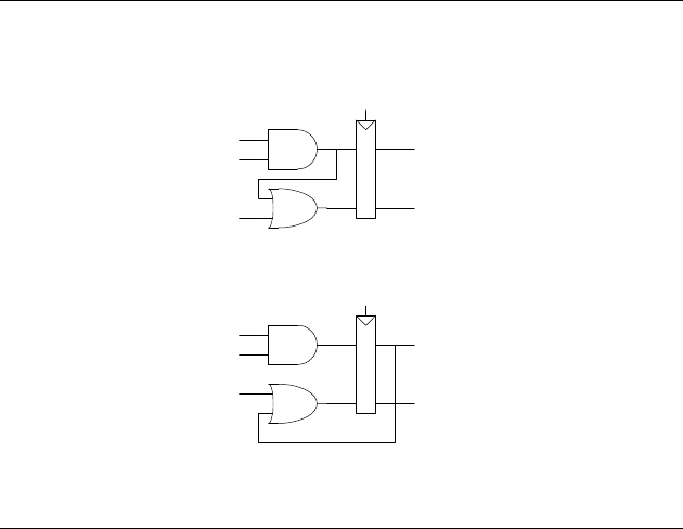
108 SOLUTIONS chapter 4
Sarah L.
Harris and David Money Harris, Digital Design and Computer Architecture: ARM® Edition © 2015
by Elsevier Inc. Exercise Solutions
Exercise 4.49
They do not have the same function.
Exercise 4.51
It is necessary to write
SystemVerilog
module syncbad(input logic clk,
input logic d,
output logic q);
logic n1;
always_ff @(posedge clk)
begin
q <= n1;// nonblocking
n1 <= d; // nonblocking
end
endmodule
VHDL
library IEEE; use IEEE.STD_LOGIC_1164.all;
entity syncbad is
port(clk: in STD_LOGIC;
d: in STD_LOGIC;
q: out STD_LOGIC);
end;
architecture bad of syncbad is
begin
process(clk)
variable n1: STD_LOGIC;
begin
if rising_edge(clk) then
q <= n1; -- nonblocking
n1 <= d; -- nonblocking
end if;
end process;
end;
B
A
CLK
X
C
Y
code1
code2
B
A
CLK
X
CY

SOLUTIONS 109
Sarah L. Harris and David Money Harris, Digital Design and Computer Architecture: ARM® Edition © 2015 by Elsevier
Inc. Exercise Solutions
q <= '1' when state = S0 else '0';
rather than simply
q <= (state = S0);
because the result of the comparison (state = S0) is of type Boolean
(true and false) and q must be assigned a value of type STD_LOGIC ('1'
and '0').
Question 4.1
Question 4.3
The SystemVerilog statement performs the bit-wise AND of the 16 least
significant bits of data with 0xC820. It then ORs these 16 bits to produce the 1-
bit result.
SystemVerilog
assign result = sel ? data : 32'b0;
VHDL
result <= data when sel = '1' else X"00000000";

SOLUTIONS 139
Sarah L. Harris and David Money Harris, Digital Design and Computer Architecture: ARM® Edition © 2015 by Elsevier
Inc. Exercise Solutions
CHAPTER 5
Exercise 5.1
(a) From Equation 5.1, we find the 64-bit ripple-carry adder delay to be:
(b) From Equation 5.6, we find the 64-bit carry-lookahead adder delay to
be:
(Note: the actual delay is only 7.2 ns because the first AND_OR gate only
has a 150 ps delay.)
(c) From Equation 5.11, we find the 64-bit prefix adder delay to be:
Exercise 5.3
A designer might choose to use a ripple-carry adder instead of a carry-loo-
kahead adder if chip area is the critical resource and delay is not the critical con-
straint.
t
ripple
Nt
FA
64 450 ps28.8 ns== =
t
CLA
t
pg
t
pg_block
N
k
----
1–
t
AND_OR
kt
FA
++ +=
t
CLA
150 6 150
64
4
------
1–
300 4 450++ + 7.35 ns==
t
PA
t
pg
Nt
pg_prefix
t
XOR
+
2
log+=
t
PA
150 6 300150++2.1 ns==

140 SOLUTIONS chapter 5
Sarah L. Harris and David Money Harris, Digital Design and Computer Architecture: ARM® Edition © 2015
by
Elsevier Inc. Exercise Solutions
Exercise 5.5
FIGURE 5.1 16-bit prefix adder with “gray cells”
Exercise 5.7
(a) We show an 8-bit priority circuit in Figure 5.2. In the figure X
7
= A
7
,
X
7:6
= A
7
A
6
, X
7:5
= A
7
A
6
A
5
, and so on. The priority encoder’s delay is log
2
N 2-
input AND gates followed by a final row of 2-input AND gates. The final stage
is an (N/2)-input OR gate. Thus, in general, the delay of an N-input priority en-
coder is:
t
pd_priority
= (log
2
N+1)t
pd_AND2
+ t
pd_ORN/2
0:-1
-1
2:1
1:-12:-1
012
4:3
3
6:5
5:36:3
456
5:-16:-1 3:-14:-1
8:7
7
10:9
9:710:7
8910
12:11
11
14:13
13:1114:11
121314
13:714:7 11:712:7
9:-110:-1 7:-18:-113:-114:-1 11:-112:-1
15
0123456789101112131415
B
i
A
i
G
i:i
P
i:i
G
k-1:j
P
k-1:j
G
i:k
P
i:k
G
i:j
P
i:j
i
i:j
B
i
A
i
G
i-1:-1
S
i
iLegend
G
k-1:j
G
i:k
P
i:k
G
i:j
i:j

SOLUTIONS 141
Sarah L. Harris and David Money Harris, Digital Design and Computer Architecture: ARM® Edition © 2015 by Elsevier
Inc. Exercise Solutions
FIGURE 5.2 8-input priority encoder
Y
0
Y
1
Y
2
Y
3
Y
4
Y
5
Y
6
Y
7
A
0
A
1
A
2
A
3
A
4
A
5
A
6
A
7
A
0
A
1
A
2
A
3
A
4
A
5
A
6
A
7
X
7:6
X
7
X
7:5
X
7:4
X
7:3
X
7:2
X
7:1
Z
0
Z
2
Z
3
Y
1
Y
3
Y
5
Y
7
Y
2
Y
3
Y
6
Y
7
Y
4
Y
5
Y
6
Y
7

142 SOLUTIONS chapter 5
Sarah L. Harris and David Money Harris, Digital Design and Computer Architecture: ARM® Edition © 2015
by Elsevier Inc. Exercise Solutions
Exercise 5.9
SystemVerilog
module priorityckt(input logic [7:0] a,
ou
tput logic [2:0] z);
logic [7:0] y;
logic x7, x76, x75, x74, x73, x72, x71;
logic x32, x54, x31;
logic [7:0] abar;
// row of inverters
assign abar = ~a;
// first row of AND gates
assign x7 = abar[7];
assign x76 = abar[6] & x7;
assign x54 = abar[4] & abar[5];
assign x32 = abar[2] & abar[3];
// second row of AND gates
assign x75 = abar[5] & x76;
assign x74 = x54 & x76;
assign x31 = abar[1] & x32;
// third row of AND gates
assign x73 = abar[3] & x74;
assign x72 = x32 & x74;
assign x71 = x31 & x74;
// fourth row of AND gates
assign y = {a[7], a[6] & x7, a[5] & x76,
a[4] & x75, a[3] & x74, a[2] & x73,
a[1] & x72, a[0] & x71};
// row of OR gates
assign z = { |{y[7:4]},
|{y[7:6], y[3:2]},
|{y[1], y[3], y[5], y[7]} };
endmodule
VHDL
library IEEE; use IEEE.STD_LOGIC_1164.all;
entity priorityckt is
port(a: in STD_LOGIC_VECTOR(7 downto 0);
z: out STD_LOGIC_VECTOR(2 downto 0));
end;
architecture synth of priorityckt is
signal y, abar: STD_LOGIC_VECTOR(7 downto 0);
signal x7, x76, x75, x74, x73, x72, x71,
x32, x54, x31: STD_LOGIC;
begin
-- row of inverters
abar <= not a;
-- first row of AND gates
x7 <= abar(7);
x76 <= abar(6) and x7;
x54 <= abar(4) and abar(5);
x32 <= abar(2) and abar(3);
-- second row of AND gates
x75 <= abar(5) and x76;
x74 <= x54 and x76;
x31 <= abar(1) and x32;
-- third row of AND gates
x73 <= abar(3) and x74;
x72 <= x32 and x74;
x71 <= x31 and x74;
-- fourth row of AND gates
y <= (a(7) & (a(6) and x7) & (a(5) and x76) &
(a(4) and x75) & (a(3) and x74) & (a(2) and
x73) &
(a(1) and x72) & (a(0) and x71));
-- row of OR gates
z <= ( (y(7) or y(6) or y(5) or y(4)) &
(y(7) or y(6) or y(3) or y(2)) &
(y(1) or y(3) or y(5) or y(7)) );
end;

143 SOLUTIONS chapter 5 S. Harris and D.M. Harris, DDCA: ARM® Edition © 2015 Elsevier, Inc.
(a) Answers will vary.
3 and 5: 3 – 5 = 0011
2
– 0101
2
= 0011
2
+ 1010
2
+ 1 = 1110
2
(= -2
10
). The sign bit (most
significant bit) is 1, so the 4-bit signed comparator of Figure 5.12 correctly computes
that 3 is less than 5.
(b) Answers will vary.
-3 and 6: -3 – 6 = 1101 – 0110 = 1101 + 1001 + 1 = 01112 (= -7, but overflow occurred –
the result should be -9). The sign bit (most significant bit) is 0, so the 4-bit signed
comparator of Figure 5.12 incorrectly computes that -3 is not less than 6.
(c) In the general, the N-
bit signed comparator of Figure 5.12 operates incorrectly upon
overflow.
Exercise 5.11
SystemVerilog
module alu(input logic [31:0] a, b,
input logic [1:0] ALUControl,
output logic [31:0] Result);
logic [31:0] condinvb;
logic [32:0] sum;
assign condinvb = ALUControl[0] ? ~b : b;
assign sum = a + condinvb + ALUControl[0];
always_comb
casex (ALUControl[1:0])
2'b0?: Result = sum;
2'b10: Result = a & b;
2'b11: Result = a | b;
endcase
endmodule
VHDL
library IEEE; use IEEE.STD_LOGIC_1164.all;
use IEEE.NUMERIC_STD_UNSIGNED.all;
entity alu is
port(a, b: in STD_LOGIC_VECTOR(31 downto 0);
ALUControl: in STD_LOGIC_VECTOR(1 downto 0);
Result: buffer STD_LOGIC_VECTOR(31 downto 0));
end;
architecture behave of alu is
signal condinvb: STD_LOGIC_VECTOR(31 downto 0);
signal sum: STD_LOGIC_VECTOR(32 downto 0);
begin
condinvb <= not b when ALUControl(0) else b;
sum <= ('0', a) + ('0', condinvb) + ALUControl(0);
process(all) begin
case? ALUControl(1 downto 0) is
when "0-" => result <= sum(31 downto 0);
when "10" => result <= a and b;
when "11" => result <= a or b;
when others => result <= (others => '-');
end case?;

144 SOLUTIONS chapter 5 S. Harris and D.M. Harris, DDCA: ARM® Edition © 2015 Elsevier, Inc.
end process;
end;
Exercise 5.13
SystemVerilog
module testbench();
logic clk;
logic [31:0] a, b, y, y_expected;
logic [1:0] ALUControl;
logic [31:0] vectornum, errors;
logic [99:0] testvectors[10000:0];
// instantiate device under test
alu dut(a, b, ALUControl, y);
// generate clock
always begin
clk = 1; #50; clk = 0; #50;
end
// at start of test, load vectors
initial begin
$readmemh("ex5.13_alu.tv", testvectors);
vectornum = 0; errors = 0;
end
// apply test vectors at rising edge of clock
always @(posedge clk)
begin
#1;
ALUControl = testvectors[vectornum][97:96];
a = testvectors[vectornum][95:64];
b = testvectors[vectornum][63:32];
y_expected = testvectors[vectornum][31:0];
end
// check results on falling edge of clock
always @(negedge clk)
begin
if (y !== y_expected) begin
$display("Error in vector %d", vectornum);
$display(" Inputs : a = %h, b = %h, ALUControl = %b", a, b, ALUControl);
$display(" Outputs: y = %h (%h expected)",
y, y_expected);
errors = errors+1;
end
vectornum = vectornum + 1;
if (testvectors[vectornum][0] === 1'bx) begin
$display("%d tests completed with %d errors", vectornum, errors);
$stop;
end
end
endmodule
VHD
L
library IEEE;
u
se IEEE.STD_LOGIC_1164.all; use STD.TEXTIO.all;
use IEEE.STD_LOGIC_UNSIGNED.all;
use IEEE.STD_LOGIC_ARITH.all;
145 SOLUTIONS chapter 5 S. Harris and D.M. Harris, DDCA: ARM® Edition © 2015 Elsevier, Inc.
entity testbench is -- no inputs or outputs
end;
architecture sim of testbench is
component alu
port(a, b: in STD_LOGIC_VECTOR(31 downto 0);
ALUControl: in STD_LOGIC_VECTOR(1 downto 0);
Result: buffer STD_LOGIC_VECTOR(31 downto 0));
end component;
signal a, b, Result, Result_expected: STD_LOGIC_VECTOR(31 downto 0);
signal ALUControl: STD_LOGIC_VECTOR(1 downto 0);
signal clk, reset: STD_LOGIC;
constant MEMSIZE: integer := 99;
type tvarray is array(MEMSIZE downto 0) of STD_LOGIC_VECTOR(99 downto 0);
shared variable testvectors: tvarray;
shared variable vectornum, errors: integer;
begin
-- instantiate device under test
dut: alu port map(a, b, ALUControl, Result);
-- generate clock
process begin
clk <= '1'; wait for 5 ns;
clk <= '0'; wait for 5 ns;
end process;
-- at start of test, pulse reset
process begin
reset <= '1'; wait for 27 ns; reset <= '0';
wait;
end process;
-- run tests
-- at start of test, load vectors
process is
file tv: TEXT;
variable i, index, count: integer;
variable L: line;
variable ch: character;
variable readvalue: integer;
begin
-- read file of test vectors
i := 0;
index := 0;
FILE_OPEN(tv, "ex5.13_alu.tv", READ_MODE);
report "Opening file\n";
while (not endfile(tv)) loop
readline(tv, L);
readvalue := 0;
count := 3;
for i in 1 to 28 loop
read(L, ch);
report "Line: " & integer'image(index) & " i = " &
integer'image(i) & " char = " &
character'image(ch)
severity error;
if '0' <= ch and ch <= '9' then
readvalue := readvalue*16 + character'pos(ch)
- character'pos('0');
elsif 'a' <= ch and ch <= 'f' then
readvalue := readvalue*16 + character'pos(ch)
- character'pos('a')+10;
146 SOLUTIONS chapter 5 S. Harris and D.M. Harris, DDCA: ARM® Edition © 2015 Elsevier, Inc.
else report "Format error on line " &
integer'image(index) & " i = " &
integer'image(i) & " char = " &
character'image(ch)
severity error;
end if;
-- load vectors
-- assign first 4 bits (will be used for ALUControl)
if (i = 1) then
testvectors(index)( 99 downto 96) := CONV_STD_LOGIC_VECTOR(readvalue, 4);
count := count - 1;
readvalue := 0; -- reset readvalue
-- assign a, b, and Result (in testvectors) in
-- 32-bit increments
elsif ((i = 10) or (i = 19) or (i = 28)) then
testvectors(index)( (count*32 + 31) downto (count*32)) :=
CONV_STD_LOGIC_VECTOR(readvalue, 32);
count := count - 1;
readvalue := 0; -- reset readvalue
end if;
end loop;
index := index + 1;
end loop;
vectornum := 0; errors := 0;
reset <= '1'; wait for 27 ns; reset <= '0';
wait;
end process;
-- apply test vectors on rising edge of clk
process (clk) begin
if (clk'event and clk = '1') then
ALUControl <= testvectors(vectornum)(97 downto 96)
after 1 ns;
a <= testvectors(vectornum)(95 downto 64)
after 1 ns;
b <= testvectors(vectornum)(63 downto 32)
after 1 ns;
Result_expected <= testvectors(vectornum)(31 downto 0)
after 1 ns;
end if;
end process;
-- check results on falling edge of clk
process (clk) begin
if (clk'event and clk = '0' and reset = '0') then
if (is_x(testvectors(vectornum))) then
if (errors = 0) then
report "Just kidding -- " & integer'image(vectornum) & " tests completed
successfully. NO ERRORS." severity failure;
else
report integer'image(vectornum) & " tests completed, errors = " &
integer'image(errors) severity failure;
end if;
end if;
assert Result = Result_expected
report "Error: vectornum = " &
integer'image(vectornum) &
", a = " & integer'image(CONV_INTEGER(a)) &

147 SOLUTIONS chapter 5 S. Harris and D.M. Harris, DDCA: ARM® Edition © 2015 Elsevier, Inc.
", b = " & integer'image(CONV_INTEGER(b)) &
", Result = " & integer'image(CONV_INTEGER(Result)) &
", ALUControl = " & integer'image(CONV_INTEGER(ALUControl));
if (Result /= Result_expected) then
errors := errors + 1;
end if;
vectornum := vectornum + 1;
end if;
end process;
end;
Testvector file (ex5.13_alu.tv)
0_00000000_00000000_00000000
0_00000000_ffffffff_ffffffff
0_00000001_ffffffff_00000000
0_000000ff_00000001_00000100
1_00000000_00000000_00000000
1_00000000_ffffffff_00000001
1_00000001_00000001_00000000
1_00000100_00000001_000000ff
2_ffffffff_ffffffff_ffffffff
2_ffffffff_12345678_12345678
2_12345678_87654321_02244220
2_00000000_ffffffff_00000000
3_ffffffff_ffffffff_ffffffff
3_12345678_87654321_97755779
3_00000000_ffffffff_ffffffff
3_00000000_00000000_00000000
Exercise 5.15
(a) =
= +
̅
=
̅
=
=
̅
=
(b)
Exercise 5.17
CZ
HS
LS
HI
LO

Sarah L. Harris and David Money Harris, Digital Design and Computer Architecture: ARM® Edition © 2015 by Elsevier
Inc. Exercise Solutions
SOLUTIO NS 148
A 2-bit left shifter creates the output by appending two zeros to the least
significant bits of the input and dropping the two most significant bits.
FIGURE 5.3 2-bit left shifter, 32-bit input and output
2-bit Left Shifter
Exercise 5.19
A
31
...
A
30
A
29
A
28
A
3
A
2
A
1
A
0
...
Y
31
Y
30
Y
5
Y
4
Y
3
Y
2
Y
1
Y
0
...
SystemVerilog
module leftshift2_32(input logic [31:0] a,
output logic [31:0] y);
assign y = {a[29:0], 2'b0};
endmodule
VHDL
library IEEE;
use IEEE.STD_LOGIC_1164.all;
entity leftshift2_32 is
port(a: in STD_LOGIC_VECTOR(31 downto 0);
y: out STD_LOGIC_VECTOR(31 downto 0));
end;
architecture synth of leftshift2_32 is
begin
y <= a(29 downto 0) & "00";
end;

Sarah L. Harris and David Money Harris, Digital Design and Computer Architecture: ARM® Edition ©
2015 by Elsevier Inc. Exercise Solutions
149 SOLU TIONS chapt er 5
FIGURE 5.4 8-bit left shifter using 24 2:1 multiplexers
Exercise 5.21
(a) B = 0, C = A, k = shamt
A
7
A
6
A
5
A
4
0
1
0
1
0
1
0
1
0
1
0
1
0
1
0
1
0
1
0
1
0
1
0
1
A
3
A
2
A
1
A
0
Y
7
Y
5
Y
3
Y
1
A
6
A
5
A
4
A
3
0
1
0
1
0
1
0
1
0
1
0
1
0
1
0
1
0
1
0
1
0
1
0
1
A
2
A
1
A
0
Y
6
Y
4
Y
2
Y
0
shamt
0
shamt
1
shamt
2

Sarah L. Harris and David Money Harris, Digital Design and Computer Architecture: ARM® Edition © 2015 by Elsevier
Inc. Exercise Solutions
SOLUTIO NS 150
(b) B = A
N-1
(the most significant bit of A), repeated N times to fill all N bits
of B
(c) B = A, C = 0, k = N - shamt
(d) B = A, C = A, k = shamt
(e) B = A, C = A, k = N - shamt
Exercise 5.23
t
pd_DIV4
= 4 (4t
FA
+ t
MUX
) = 16t
FA
+ 4t
MUX
t
pd_DIVN
= N
2
t
FA
+ Nt
MUX
Exercise 5.25
FIGURE 5.5 Sign extension unit (a) symbol, (b) underlying hardware
A
3
A
2
A
1
A
0
Y
3
Y
2
Y
1
Y
0
Y
7
Y
6
Y
5
Y
4
Sign Extend
48
(a) (b)
A
3:0
Y
7:0
SystemVerilog
module signext4_8(input logic [3:0] a,
output logic [7:0] y);
assign y = { {4{a[3]}}, a};
endmodule
VHDL
library IEEE;
use IEEE.STD_LOGIC_1164.all;
entity signext4_8 is
port(a: in STD_LOGIC_VECTOR(3 downto 0);
y: out STD_LOGIC_VECTOR(7 downto 0));
end;
architecture synth of signext4_8 is
begin

Sarah L. Harris and David Money Harris, Digital Design and Computer Architecture: ARM® Edition ©
2015 by Elsevier Inc. Exercise Solutions
151 SOLU TIONS chapt er 5
Exercise 5.27
Exercise 5.29
(a) 1000 1101 . 1001 0000 = 0x8D90
(b) 0010 1010 . 0101 0000 = 0x2A50
(c) 1001 0001 . 0010 1000 = 0x9128
Exercise 5.31
(a) 1111 0010 . 0111 0000 = 0xF270
(b) 0010 1010 . 0101 0000 = 0x2A50
(c) 1110 1110 . 1101 1000 = 0xEED8
Exercise 5.33
(a) -1101.1001 = -1.1011001 2
3
Thus, the biased exponent = 127 + 3 = 130 = 1000 0010
2
In IEEE 754 single-precision floating-point format:
1 1000 0010 101 1001 0000 0000 0000 0000 = 0xC1590000
(b) 101010.0101 = 1.010100101
2
5
Thus, the biased exponent = 127 + 5 = 132 = 1000 0100
2
In IEEE 754 single-precision floating-point format:
0 1000 0100 010 1001 0100 0000 0000 0000 = 0x42294000
(c) -10001.00101 = -1.000100101
2
4
Thus, the biased exponent = 127 + 4 = 131 = 1000 0011
2
In IEEE 754 single-precision floating-point format:
1 1000 0011 000 1001 0100 0000 0000 0000 = 0xC1894000
111001.000
001001 0
1100
1100
100.110
110 0
-
-
11 00
11 00
-
0

SOLUTIONS 152
Sarah L. Harris and David Money Harris, Digital Design and Computer Architecture: ARM® Edition © 2015 by Elsevier
Inc. Exercise Solutions
Exercise 5.35
(a) 5.5
(b) -0000.0001
2
= -0.0625
(c) -8
Exercise 5.37
When adding two floating point numbers, the number with the smaller ex-
ponent is shifted to preserve the most significant bits. For example, suppose we
were adding the two floating point numbers 1.0
2
0
and 1.0 2
-27
. We make
the two exponents equal by shifting the second number right by 27 bits. Because
the mantissa is limited to 24 bits, the second number (1.000 0000 0000 0000
0000
2
-27
) becomes 0.000 0000 0000 0000 0000 2
0
, because the 1 is shifted
off to the right. If we had shifted the number with the larger exponent (1.0
2
0
)
to the left, we would have shifted off the more significant bits (on the order of
2
0
instead of on the order of 2
-27
).
Exercise 5.39
(a)
0xC0D20004 = 1 1000 0001 101 0010 0000 0000 0000 0100
= - 1.101 0010 0000 0000 0000 01
2
2
0x72407020 = 0 1110 0100 100 0000 0111 0000 0010 0000
= 1.100 0000 0111 0000 001
2
101
When adding these two numbers together, 0xC0D20004 becomes:
0
2
101
because all of the significant bits shift off the right when making
the exponents equal. Thus, the result of the addition is simply the second num-
ber:
0x72407020
(b)
0xC0D20004 = 1 1000 0001 101 0010 0000 0000 0000 0100
= - 1.101 0010 0000 0000 0000 01
2
2
0x40DC0004 = 0 1000 0001 101 1100 0000 0000 0000 0100
= 1.101 1100 0000 0000 0000 01
2
2
1.101 1100 0000 0000 0000 01 2
2

153 SOLUTIONS chapter 5
Sarah L. Harris and David Money Harris, Digital Design and Computer Architecture: ARM® Edition © 2015
by Elsevier Inc. Exercise Solutions
- 1.101 0010 0000 0000 0000 01 2
2
= 0.000 1010 2
2
= 1.010 2
-2
= 0 0111 1101 010 0000 0000 0000 0000 0000
= 0x3EA00000
(c)
0x5FBE4000 = 0 1011 1111 011 1110 0100 0000 0000 0000 0000
= 1.011 1110 01
2
64
0x3FF80000 = 0 0111 1111 111 1000 0000 0000 0000 0000
= 1.111 1
2
0
0xDFDE4000 = 1 1011 1111 101 1110 0100 0000 0000 0000 0000
= - 1.101 1110 01
2
64
Thus, (1.011 1110 01 2
64
+ 1.111 1 2
0
) = 1.011 1110 01 2
64
And, (1.011 1110 01 2
64
+ 1.111 1 2
0
) - 1.101 1110 01 2
64
=
- 0.01
2
64
= -1.0 2
64
= 1 1011 1101 000 0000 0000 0000 0000 0000
= 0xDE800000
This is counterintuitive because the second number (0x3FF80000) does not
affect the result because its order of magnitude is less than 2
23
of the other num-
bers. This second number’s significant bits are shifted off when the exponents
are made equal.
Exercise 5.41
(a) 2(2
31
- 1 - 2
23
) = 2
32
- 2 - 2
24
= 4,278,190,078
(b) 2(2
31
- 1) = 2
32
- 2 = 4,294,967,294
(c)
and NaN are given special representations because they are often used in
calculations and in representing results. These values also give useful information to the
user as return values, instead of returning garbage upon overflow, underflow, or divide
by zero.
Exercise 5.43

SOLUTIONS 154
Sarah L. Harris and David Money Harris, Digital Design and Computer Architecture: ARM® Edition © 2015 by Elsevier
Inc. Exercise Solutions
FIGURE 5.6 Floating-point adder hardware: (a) block diagram, (b) underlying hardware
-
32
[30:23] [22:0]
A
31:0
ExpA
7:0
MantA
23:0
ExpB
7:0
ExpA
7:0
-
[7]
24
32
[30:23] [22:0]
B
31:0
ExpB
7:0
MantB
23:0
24
0
1
shamt
7:0
ExpA < ExpB
Exponent
Compare
ExpB
7:0
ExpA
7:0
8 8
8 8
Exp
7:0
shamt
7:0
ExpA<ExpB
Shift
Mantissa
MantA
23:0
MantB
23:0
24 24
24
ExpA<ExpB
Add Mantissas
and Normalize
MantA
23:0
MantB
23:0
24 24
24
Fract
22:0
ExpA<ExpB
24
S
31:0
32
[30:23] [22:0][31]
0
1
Exp
7:0
>>
[4:0]
0
1
MantA
23:0
MantB
23:0
ExpA < ExpB shamt
7:0
24
ShiftedMant
23:0
0
1
shamt
7:0
[7]
[6]
[5]
[4]
[3]
24 24
+
0
1
0
1
MantB
23:0
MantA
23:0
ExpA < ExpB
ShiftedMant
23:0
ShiftedMant
23:0
ShiftedMant
23:0
[23:1] [22:0]
25
[24]
23
Fract
22:0
Exp
7:0
Fract
22:0
Exponent Compare Shift Mantissa Add Mantissas and Normalize
(a) (b)
155 SOLUTIONS chapter 5
Sarah L. Harris and David Money Harris, Digital Design and Computer Architecture: ARM® Edition © 2015
by Elsevier Inc. Exercise Solutions
SystemVerilog
module fpadd(input logic [31:0] a, b,
output logic [31:0] s);
logic [7:0] expa, expb, exp_pre, exp, shamt;
logic alessb;
logic [23:0] manta, mantb, shmant;
logic [22:0] fract;
assign {expa, manta} = {a[30:23], 1'b1, a[22:0]};
assign {expb, mantb} = {b[30:23], 1'b1, b[22:0]};
assign s = {1'b0, exp, fract};
expcomp expcomp1(expa, expb, alessb, exp_pre,
shamt);
shiftmant shiftmant1(alessb, manta, mantb,
shamt, shmant);
addmant addmant1(alessb, manta, mantb,
shmant, exp_pre, fract, exp);
endmodule
VHDL
library IEEE; use IEEE.STD_LOGIC_1164.all;
use IEEE.STD_LOGIC_UNSIGNED.all;
use IEEE.STD_LOGIC_ARITH.all;
entity fpadd is
port(a, b: in STD_LOGIC_VECTOR(31 downto 0);
s: out STD_LOGIC_VECTOR(31 downto 0));
end;
architecture synth of fpadd is
component expcomp
port(expa, expb: in STD_LOGIC_VECTOR(7 downto 0);
alessb: inout STD_LOGIC;
exp,shamt: out STD_LOGIC_VECTOR(7 downto 0));
end component;
component shiftmant
port(alessb: in STD_LOGIC;
manta: in STD_LOGIC_VECTOR(23 downto 0);
mantb: in STD_LOGIC_VECTOR(23 downto 0);
shamt: in STD_LOGIC_VECTOR(7 downto 0);
shmant: out STD_LOGIC_VECTOR(23 downto 0));
end component;
component addmant
port(alessb: in STD_LOGIC;
manta: in STD_LOGIC_VECTOR(23 downto 0);
mantb: in STD_LOGIC_VECTOR(23 downto 0);
shmant: in STD_LOGIC_VECTOR(23 downto 0);
exp_pre: in STD_LOGIC_VECTOR(7 downto 0);
fract: out STD_LOGIC_VECTOR(22 downto 0);
exp: out STD_LOGIC_VECTOR(7 downto 0));
end component;
signal expa, expb: STD_LOGIC_VECTOR(7 downto 0);
signal exp_pre, exp: STD_LOGIC_VECTOR(7 downto 0);
signal shamt: STD_LOGIC_VECTOR(7 downto 0);
signal alessb: STD_LOGIC;
signal manta: STD_LOGIC_VECTOR(23 downto 0);
signal mantb: STD_LOGIC_VECTOR(23 downto 0);
signal shmant: STD_LOGIC_VECTOR(23 downto 0);
signal fract: STD_LOGIC_VECTOR(22 downto 0);
begin
expa <= a(30 downto 23);
manta <= '1' & a(22 downto 0);
expb <= b(30 downto 23);
mantb <= '1' & b(22 downto 0);
s <= '0' & exp & fract;
expcomp1: expcomp
port map(expa, expb, alessb, exp_pre, shamt);
shiftmant1: shiftmant
port map(alessb, manta, mantb, shamt, shmant);
addmant1: addmant
port map(alessb, manta, mantb, shmant,
exp_pre, fract, exp);
end;
SOLUTIONS 156
Sarah L. Harris and David Money Harris, Digital Design and Computer Architecture: ARM® Edition © 2015 by Elsevier
Inc. Exercise Solutions
(continued from previous page)
(continued on next page)
SystemVerilog
module expcomp(input logic [7:0] expa, expb,
output logic alessb,
output logic [7:0] exp, shamt);
logic [7:0] aminusb, bminusa;
assign aminusb = expa - expb;
assign bminusa = expb - expa;
assign alessb = aminusb[7];
always_comb
if (alessb) begin
exp = expb;
shamt = bminusa;
end
else begin
exp = expa;
shamt = aminusb;
end
endmodule
VHDL
library IEEE; use IEEE.STD_LOGIC_1164.all;
use IEEE.STD_LOGIC_UNSIGNED.all;
use IEEE.STD_LOGIC_ARITH.all;
entity expcomp is
port(expa, expb: in STD_LOGIC_VECTOR(7 downto 0);
alessb: inout STD_LOGIC;
exp,shamt: out STD_LOGIC_VECTOR(7 downto 0));
end;
architecture synth of expcomp is
signal aminusb: STD_LOGIC_VECTOR(7 downto 0);
signal bminusa: STD_LOGIC_VECTOR(7 downto 0);
begin
aminusb <= expa - expb;
bminusa <= expb - expa;
alessb <= aminusb(7);
exp <= expb when alessb = '1' else expa;
shamt <= bminusa when alessb = '1' else aminusb;
end;
157 SOLUTIONS chapter 5
Sarah L. Harris and David Money Harris, Digital Design and Computer Architecture: ARM® Edition © 2015
by Elsevier Inc. Exercise Solutions
(continued from previous page)
SystemVerilog
module shiftmant(input logic alessb,
input logic [23:0] manta, mantb,
input logic [7:0] shamt,
output logic [23:0] shmant);
logic [23:0] shiftedval;
assign shiftedval = alessb ?
(manta >> shamt) : (mantb >> shamt);
always_comb
if (shamt[7] | shamt[6] | shamt[5] |
(shamt[4] & shamt[3]))
shmant = 24'b0;
else
shmant = shiftedval;
endmodule
module addmant(input logic alessb,
input logic [23:0] manta,
mantb, shmant,
input logic [7:0] exp_pre,
output logic [22:0] fract,
output logic [7:0] exp);
logic [24:0] addresult;
logic [23:0] addval;
assign addval = alessb ? mantb : manta;
assign addresult = shmant + addval;
assign fract = addresult[24] ?
addresult[23:1] :
addresult[22:0];
assign exp
= addresult[24] ?
(exp_pre + 1) :
exp_pre;
endmodule
VHDL
library IEEE; use IEEE.STD_LOGIC_1164.all;
use ieee.numeric_std.all;
use IEEE.std_logic_unsigned.all;
entity shiftmant is
port(alessb: in STD_LOGIC;
manta: in STD_LOGIC_VECTOR(23 downto 0);
mantb: in STD_LOGIC_VECTOR(23 downto 0);
s
hamt: in STD_LOGIC_VECTOR(7 downto 0);
shmant: out STD_LOGIC_VECTOR(23 downto 0));
end;
architecture synth of shiftmant is
signal shiftedval: unsigned (23 downto 0);
signal shiftamt_vector: STD_LOGIC_VECTOR (7 downto
0);
begin
shiftedval <= SHIFT_RIGHT( unsigned(manta), to_in-
teger(unsigned(shamt))) when alessb = '1'
else SHIFT_RIGHT( unsigned(mantb), to_in-
teger(unsigned(shamt)));
shmant <= X"000000" when (shamt > 22)
else STD_LOGIC_VECTOR(shiftedval);
end;
library IEEE; use IEEE.STD_LOGIC_1164.all;
use IEEE.STD_LOGIC_UNSIGNED.all;
use IEEE.STD_LOGIC_ARITH.all;
entity addmant is
port(alessb: in STD_LOGIC;
manta: in STD_LOGIC_VECTOR(23 downto 0);
mantb: in STD_LOGIC_VECTOR(23 downto 0);
shmant: in STD_LOGIC_VECTOR(23 downto 0);
exp_pre: in STD_LOGIC_VECTOR(7 downto 0);
fract: out STD_LOGIC_VECTOR(22 downto 0);
exp: out STD_LOGIC_VECTOR(7 downto 0));
end;
architecture synth of addmant is
signal addresult: STD_LOGIC_VECTOR(24 downto 0);
signal addval: STD_LOGIC_VECTOR(23 downto 0);
begin
addval <= mantb when alessb = '1' else manta;
addresult <= ('0'&shmant) + addval;
fract <= addresult(23 downto 1)
when addresult(24) = '1'
else addresult(22 downto 0);
exp <= (exp_pre + 1)
when addresult(24) = '1'
else exp_pre;
end;

SOLUTIONS 158
Sarah L. Harris and David Money Harris, Digital Design and Computer Architecture: ARM® Edition © 2015 by Elsevier
Inc. Exercise Solutions
Exercise 5.45
(a) Figure on next page

SOLUTIONS 159
Sarah L. Harris and David Money Harris, Digital Design and Computer Architecture: ARM® Edition © 2015 by Elsevier
Inc. Exercise Solutions
16:15
15
18:17
17:1518:15
161718
20:19
19
22:21
21:1922:19
202122
21:1522:15 19:1520:15
24:2326:25
25:2326:23
242526
28:27
27
30:29
29:2730:27
282930
29:2330:23 27:2328:23
25:1526:15 23:1524:1529:1530:15 27:1528:15
31
16171819202122232425262728293031
B
i
A
i
G
i:i
P
i:i
G
k-1:j
P
k-1:j
G
i:k
P
i:k
G
i:j
P
i:j
i
i:j
B
i
A
i
G
i-1:-1
S
i
iLegend
23
0:-1
-1
2:1
1:-12:-1
012
4:3
3
6:5
5:36:3
456
5:-16:-1 3:-14:-1
8:7
7
10:9
9:710:7
8910
12:11
11
14:13
13:1114:11
121314
13:714:7 11:712:7
9:-110:-1 7:-18:-113:-114:-1 11:-112:-1
0123456789101112131415
25:-126:-1 23:-124:-129:-130:-1 27:-128:-1 18:-1 15:-116:-121:-122:-1 19:-120:-1 17:-1
Row 1
Row 2
Row 3
Row 4
Row 5
160 SOLUTIONS chapter 5
Sarah L. Harris and David Money Harris, Digital Design and Computer Architecture: ARM® Edition © 2015
by Elsevier Inc. Exercise Solutions
5.45 (b)
SystemVerilog
module prefixadd(input logic [31:0] a, b,
input logic cin,
output logic [31:0] s,
output logic
cout);
logic [30:0] p, g;
// p and g prefixes for rows 1 - 5
logic [15:0] p1, p2, p3, p4, p5;
logic [15:0] g1, g2, g3, g4, g5;
pandg row0(a, b, p, g);
blackbox row1({p[30],p[28],p[26],p[24],p[22],
p[20],p[18],p[16],p[14],p[12],
p[10],p[8],p[6],p[4],p[2],p[0]},
{p[29],p[27],p[25],p[23],p[21],
p[19],p[17],p[15],p[13],p[11],
p[9],p[7],p[5],p[3],p[1],1'b0},
{g[30],g[28],g[26],g[24],g[22],
g[20],g[18],g[16],g[14],g[12],
g[10],g[8],g[6],g[4],g[2],g[0]},
{g[29],g[27],g[25],g[23],g[21],
g[19],g[17],g[15],g[13],g[11],
g[9],g[7],g[5],g[3],g[1],cin},
p1, g1);
VHDL
library IEEE; use IEEE.STD_LOGIC_1164.all;
entity prefixadd is
port(a, b: in STD_LOGIC_VECTOR(31 downto 0);
cin: in STD_LOGIC;
s: out STD_LOGIC_VECTOR(31 downto 0);
cout: out STD_LOGIC);
end;
architecture synth of prefixadd is
component pgblock
port(a, b: in STD_LOGIC_VECTOR(30 downto 0);
p, g: out STD_LOGIC_VECTOR(30 downto 0));
end component;
component pgblackblock is
port (pik, gik: in STD_LOGIC_VECTOR(15 downto 0);
pkj, gkj: in STD_LOGIC_VECTOR(15 downto 0);
pij: out STD_LOGIC_VECTOR(15 downto 0);
gij: out STD_LOGIC_VECTOR(15 downto 0));
end component;
component sumblock is
port (a, b, g: in STD_LOGIC_VECTOR(31 downto 0);
s: out STD_LOGIC_VECTOR(31 downto 0));
end component;
signal p, g: STD_LOGIC_VECTOR(30 downto 0);
signal pik_1, pik_2, pik_3, pik_4, pik_5,
gik_1, gik_2, gik_3, gik_4, gik_5,
pkj_1, pkj_2, pkj_3, pkj_4, pkj_5,
gkj_1, gkj_2, gkj_3, gkj_4, gkj_5,
p1, p2, p3, p4, p5,
g1, g2, g3, g4, g5:
STD_LOGIC_VECTOR(15 downto 0);
signal g6: STD_LOGIC_VECTOR(31 downto 0);
begin
row0: pgblock
port map(a(30 downto 0), b(30 downto 0), p, g);
pik_1 <=
(p(30)&p(28)&p(26)&p(24)&p(22)&p(20)&p(18)&p(16)&
p(14)&p(12)&p(10)&p(8)&p(6)&p(4)&p(2)&p(0));
gik_1 <=
(g(30)&g(28)&g(26)&g(24)&g(22)&g(20)&g(18)&g(16)&
g(14)&g(12)&g(10)&g(8)&g(6)&g(4)&g(2)&g(0));
pkj_1 <=
(p(29)&p(27)&p(25)&p(23)&p(21)&p(19)&p(17)&p(15)&
p(13)&p(11)&p(9)&p(7)&p(5)&p(3)&p(1)&'0');
gkj_1 <=
(g(29)&g(27)&g(25)&g(23)&g(21)&g(19)&g(17)&g(15)&
g(13)&g(11)&g(9)&g(7)&g(5)& g(3)& g(1)& cin);
row1: pgblackblock
port map(pik_1, gik_1, pkj_1, gkj_1,
p1, g1);
SOLUTIONS 161
Sarah L. Harris and David Money Harris, Digital Design and Computer Architecture: ARM® Edition © 2015 by Elsevier
Inc. Exercise Solutions
(continued from previous page)
(continued on next page)
SystemVerilog
blackbox row2({p1[15],p[29],p1[13],p[25],p1[11],
p[21],p1[9],p[17],p1[7],p[13],
p1[5],p[9],p1[3],p[5],p1[1],p[1]},
{{2{p1[14]}},{2{p1[12]}},{2{p1[10]}},
{2{p1[8]}},{2{p1[6]}},{2{p1[4]}},
{2{p1[2]}},{2{p1[0]}}},
{g1[15],g[29],g1[13],g[25],g1[11],
g[21],g1[9],g[17],g1[7],g[13],
g1[5],g[9],g1[3],g[5],g1[1],g[1]},
{{2{g1[14]}},{2{g1[12]}},{2{g1[10]}},
{2{g1[8]}},{2{g1[6]}},{2{g1[4]}},
{2{g1[2]}},{2{g1[0]}}},
p2, g2);
blackbox row3({p2[15],p2[14],p1[14],p[27],p2[11],
p2[10],p1[10],p[19],p2[7],p2[6],
p1[6],p[11],p2[3],p2[2],p1[2],p[3]},
{{4{p2[13]}},{4{p2[9]}},{4{p2[5]}},
{4{p2[1]}}},
{g2[15],g2[14],g1[14],g[27],g2[11],
g2[10],g1[10],g[19],g2[7],g2[6],
g1[6],g[11],g2[3],g2[2],g1[2],g[3]},
{{4{g2[13]}},{4{g2[9]}},{4{g2[5]}},
{4{g2[1]}}},
p3, g3);
VHDL
pik_2 <= p1(15)&p(29)&p1(13)&p(25)&p1(11)&
p(21)&p1(9)&p(17)&p1(7)&p(13)&
p1(5)&p(9)&p1(3)&p(5)&p1(1)&p(1);
gik_2 <= g1(15)&g(29)&g1(13)&g(25)&g1(11)&
g(21)&g1(9)&g(17)&g1(7)&g(13)&
g1(5)&g(9)&g1(3)&g(5)&g1(1)&g(1);
pkj_2 <=
p1(14)&p1(14)&p1(12)&p1(12)&p1(10)&p1(10)&
p1(8)&p1(8)&p1(6)&p1(6)&p1(4)&p1(4)&
p1(2)&p1(2)&p1(0)&p1(0);
gkj_2 <=
g1(14)&g1(14)&g1(12)&g1(12)&g1(10)&g1(10)&
g1(8)&g1(8)&g1(6)&g1(6)&g1(4)&g1(4)&
g1(2)&g1(2)&g1(0)&g1(0);
row2: pgblackblock
port map(pik_2, gik_2, pkj_2, gkj_2,
p2, g2);
pik_3 <= p2(15)&p2(14)&p1(14)&p(27)&p2(11)&
p2(10)&p1(10)&p(19)&p2(7)&p2(6)&
p1(6)&p(11)&p2(3)&p2(2)&p1(2)&p(3);
gik_3 <= g2(15)&g2(14)&g1(14)&g(27)&g2(11)&
g2(10)&g1(10)&g(19)&g2(7)&g2(6)&
g1(6)&g(11)&g2(3)&g2(2)&g1(2)&g(3);
pkj_3 <= p2(13)&p2(13)&p2(13)&p2(13)&
p2(9)&p2(9)&p2(9)&p2(9)&
p2(5)&p2(5)&p2(5)&p2(5)&
p2(1)&p2(1)&p2(1)&p2(1);
gkj_3 <= g2(13)&g2(13)&g2(13)&g2(13)&
g2(9)&g2(9)&g2(9)&g2(9)&
g2(5)&g2(5)&g2(5)&g2(5)&
g2(1)&g2(1)&g2(1)&g2(1);
row3: pgblackblock
port map(pik_3, gik_3, pkj_3, gkj_3, p3, g3);
162 SOLUTIONS chapter 5
Sarah L. Harris and David Money Harris, Digital Design and Computer Architecture: ARM® Edition © 2015
by Elsevier Inc. Exercise Solutions
(continued on next page)
SystemVerilog
blackbox row4({p3[15:12],p2[13:12],
p1[12],p[23],p3[7:4],
p2[5:4],p1[4],p[7]},
{{8{p3[11]}},{8{p3[3]}}},
{g3[15:12],g2[13:12],
g1[12],g[23],g3[7:4],
g2[5:4],g1[4],g[7]},
{{8{g3[11]}},{8{g3[3]}}},
p4, g4);
blackbox row5({p4[15:8],p3[11:8],p2[9:8],
p1[8],p[15]},
{{16{p4[7]}}},
{g4[15:8],g3[11:8],g2[9:8],
g1[8],g[15]},
{{16{g4[7]}}},
p5,g5);
sum row6({g5,g4[7:0],g3[3:0],g2[1:0],g1[0],cin},
a, b, s);
// generate cout
assign cout = (a[31] & b[31]) |
(g5[15] & (a[31] | b[31]));
endmodule
VHDL
pik_4 <= p3(15 downto 12)&p2(13 downto 12)&
p1(12)&p(23)&p3(7 downto 4)&
p2(5 downto 4)&p1(4)&p(7);
gik_4 <= g3(15 downto 12)&g2(13 downto 12)&
g1(12)&g(23)&g3(7 downto 4)&
g2(5 downto 4)&g1(4)&g(7);
pkj_4 <= p3(11)&p3(11)&p3(11)&p3(11)&
p3(11)&p3(11)&p3(11)&p3(11)&
p3(3)&p3(3)&p3(3)&p3(3)&
p3(3)&p3(3)&p3(3)&p3(3);
gkj_4 <= g3(11)&g3(11)&g3(11)&g3(11)&
g3(11)&g3(11)&g3(11)&g3(11)&
g3(3)&g3(3)&g3(3)&g3(3)&
g3(3)&g3(3)&g3(3)&g3(3);
row4: pgblackblock
port map(pik_4, gik_4, pkj_4, gkj_4, p4, g4);
pik_5 <= p4(15 downto 8)&p3(11 downto 8)&
p2(9 downto 8)&p1(8)&p(15);
gik_5 <= g4(15 downto 8)&g3(11 downto 8)&
g2(9 downto 8)&g1(8)&g(15);
pkj_5 <= p4(7)&p4(7)&p4(7)&p4(7)&
p4(7)&p4(7)&p4(7)&p4(7)&
p4(7)&p4(7)&p4(7)&p4(7)&
p4(7)&p4(7)&p4(7)&p4(7);
gkj_5 <= g4(7)&g4(7)&g4(7)&g4(7)&
g4(7)&g4(7)&g4(7)&g4(7)&
g4(7)&g4(7)&g4(7)&g4(7)&
g4(7)&g4(7)&g4(7)&g4(7);
row5: pgblackblock
port map(pik_5, gik_5, pkj_5, gkj_5, p5, g5);
g6 <= (g5 & g4(7 downto 0) & g3(3 downto 0) &
g2(1 downto 0) & g1(0) & cin);
row6: sumblock
port map(g6, a, b, s);
-- generate cout
cout <= (a(31) and b(31)) or
(g6(31) and (a(31) or b(31)));
end;
SOLUTIONS 163
Sarah L. Harris and David Money Harris, Digital Design and Computer Architecture: ARM® Edition © 2015 by Elsevier
Inc. Exercise Solutions
(continued from previous page)
SystemVerilog
module pandg(input logic [30:0] a, b,
output logic [30:0] p, g);
assign p = a | b;
assign g = a & b;
endmodule
module blackbox(input logic [15:0] pleft, pright,
gleft, gright,
output logic [15:0] pnext, gnext);
assign pnext = pleft & pright;
assign gnext = pleft & gright | gleft;
endmodule
module sum(input logic [31:0] g, a, b,
output logic [31:0] s);
assign s = a ^ b ^ g;
endmodule
VHDL
library IEEE; use IEEE.STD_LOGIC_1164.all;
entity pgblock is
port(a, b: in STD_LOGIC_VECTOR(30 downto 0);
p, g: out STD_LOGIC_VECTOR(30 downto 0));
end;
architecture synth of pgblock is
begin
p <= a or b;
g <= a and b;
end;
library IEEE; use IEEE.STD_LOGIC_1164.all;
entity pgblackblock is
port(pik, gik, pkj, gkj:
in STD_LOGIC_VECTOR(15 downto 0);
pij, gij:
out STD_LOGIC_VECTOR(15 downto 0));
end;
architecture synth of pgblackblock is
begin
pij <= pik and pkj;
gij <= gik or (pik and gkj);
end;
library IEEE; use IEEE.STD_LOGIC_1164.all;
entity sumblock is
port(g, a, b: in STD_LOGIC_VECTOR(31 downto 0);
s: out STD_LOGIC_VECTOR(31 downto 0));
end;
architecture synth of sumblock is
begin
s <= a xor b xor g;
end;
164 SOLUTIONS chapter 5
Sarah L. Harris and David Money Harris, Digital Design and Computer Architecture: ARM® Edition © 2015
by Elsevier Inc. Exercise Solutions
5.45 (c) Using Equation 5.11 to find the delay of the prefix adder:
We find the delays for each block:
t
pg
= 100 ps
t
pg_prefix
= 200 ps
t
XOR
= 100 ps
Thus,
t
PA
= [100 + 5(200) + 100] ps = 1200 ps = 1.2 ns
5.45
(d) To make a pipelined prefix adder, add pipeline registers between
each of the rows of the prefix adder. Now each stage will take 200 ps plus the
t
PA
t
pg
Nt
pg_prefix
t
XOR
+
2
log+=
SOLUTIONS 165
Sarah L. Harris and David Money Harris, Digital Design and Computer Architecture: ARM® Edition © 2015 by Elsevier
Inc. Exercise Solutions
sequencing overhead, t
pq
+ t
setup
= 80ps. Thus each cycle is 280 ps and the de-
sign can run at 3.57 GHz.

166 SOLUTIONS chapter 5
Sarah L. Harris and David Money Harris, Digital Design and Computer Architecture: ARM® Edition © 2015
by Elsevier Inc. Exercise Solutions
16:15
15
18:17
17:1518:15
161718
20:19
19
22:21
21:1922:19
202122
21:1522:15 19:1520:15
24:2326:25
25:2326:23
242526
28:27
27
30:29
29:2730:27
282930
29:2330:23 27:2328:23
25:1526:15 23:1524:1529:1530:15 27:1528:15
31
16171819202122232425262728293031
B
i
A
i
G
i:i
P
i:i
G
k-1:j
P
k-1:j
G
i:k
P
i:k
G
i:j
P
i:j
i
i:j
B
i
A
i
G
i-1:-1
S
i
iLegend
23
0:-1
-1
2:1
1:-12:-1
012
4:3
3
6:5
5:36:3
456
5:-16:-1 3:-14:-1
8:7
7
10:9
9:710:7
8910
12:11
11
14:13
13:1114:11
121314
13:714:7 11:712:7
9:-110:-1 7:-18:-113:-114:-1 11:-112:-1
0123456789101112131415
25:-126:-1 23:-124:-129:-130:-1 27:-128:-1 18:-1 15:-116:-121:-122:-1 19:-120:-1 17:-1
Register
Register
Register
Register
Register
Register
Register
SOLUTIONS 167
Sarah L. Harris and David Money Harris, Digital Design and Computer Architecture: ARM® Edition © 2015 by Elsevier
Inc. Exercise Solutions
5.45 (e)
SystemVerilog
module prefixaddpipe(input logic clk, cin,
input logic [31:0] a, b,
output logic [31:0] s, output cout);
// p and g prefixes for rows 0 - 5
logic [30:0] p0, p1, p2, p3, p4, p5;
logic [30:0] g0, g1, g2, g3, g4, g5;
logic p_1_0, p_1_1, p_1_2, p_1_3, p_1_4, p_1_5,
g_1_0, g_1_1, g_1_2, g_1_3, g_1_4, g_1_5;
// pipeline values for a and b
logic [31:0] a0, a1, a2, a3, a4, a5,
b0, b1, b2, b3, b4, b5;
// row 0
flop #(2) flop0_pg_1(clk, {1'b0,cin}, {p_1_0,g_1_0});
pandg row0(clk, a[30:0], b[30:0], p0, g0);
// row 1
flop #(2) flop1_pg_1(clk, {p_1_0,g_1_0}, {p_1_1,g_1_1});
flop #(30) flop1_pg(clk,
{p0[29],p0[27],p0[25],p0[23],p0[21],p0[19],p0[17],p0[15],
p0[13],p0[11],p0[9],p0[7],p0[5],p0[3],p0[1],
g0[29],g0[27],g0[25],g0[23],g0[21],g0[19],g0[17],g0[15],
g0[13],g0[11],g0[9],g0[7],g0[5],g0[3],g0[1]},
{p1[29],p1[27],p1[25],p1[23],p1[21],p1[19],p1[17],p1[15],
p1[13],p1[11],p1[9],p1[7],p1[5],p1[3],p1[1],
g1[29],g1[27],g1[25],g1[23],g1[21],g1[19],g1[17],g1[15],
g1[13],g1[11],g1[9],g1[7],g1[5],g1[3],g1[1]});
blackbox row1(clk,
{p0[30],p0[28],p0[26],p0[24],p0[22],
p0[20],p0[18],p0[16],p0[14],p0[12],
p0[10],p0[8],p0[6],p0[4],p0[2],p0[0]},
{p0[29],p0[27],p0[25],p0[23],p0[21],
p0[19],p0[17],p0[15],p0[13],p0[11],
p0[9],p0[7],p0[5],p0[3],p0[1],1'b0},
{g0[30],g0[28],g0[26],g0[24],g0[22],
g0[20],g0[18],g0[16],g0[14],g0[12],
g0[10],g0[8],g0[6],g0[4],g0[2],g0[0]},
{g0[29],g0[27],g0[25],g0[23],g0[21],
g0[19],g0[17],g0[15],g0[13],g0[11],
g0[9],g0[7],g0[5],g0[3],g0[1],g_1_0},
{p1[30],p1[28],p1[26],p1[24],p1[22],p1[20],
p1[18],p1[16],p1[14],p1[12],p1[10],p1[8],
p1[6],p1[4],p1[2],p1[0]},
{g1[30],g1[28],g1[26],g1[24],g1[22],g1[20],
g1[18],g1[16],g1[14],g1[12],g1[10],g1[8],
g1[6],g1[4],g1[2],g1[0]});
// row 2
flop #(2) flop2_pg_1(clk, {p_1_1,g_1_1}, {p_1_2,g_1_2});
flop #(30) flop2_pg(clk,
{p1[28:27],p1[24:23],p1[20:19],p1[16:15],p1[12:11],
168 SOLUTIONS chapter 5
Sarah L. Harris and David Money Harris, Digital Design and Computer Architecture: ARM® Edition © 2015
by Elsevier Inc. Exercise Solutions
p1[8:7],p1[4:3],p1[0],
g1[28:27],g1[24:23],g1[20:19],g1[16:15],g1[12:11],
g1[8:7],g1[4:3],g1[0]},
{p2[28:27],p2[24:23],p2[20:19],p2[16:15],p2[12:11],
p2[8:7],p2[4:3],p2[0],
g2[28:27],g2[24:23],g2[20:19],g2[16:15],g2[12:11],
g2[8:7],g2[4:3],g2[0]});
blackbox row2(clk,
{p1[30:29],p1[26:25],p1[22:21],p1[18:17],p1[14:13],p1[10:9],p1[6:5],p1[2:1]
},
{ {2{p1[28]}}, {2{p1[24]}}, {2{p1[20]}}, {2{p1[16]}}, {2{p1[12]}},
{2{p1[8]}},
{2{p1[4]}}, {2{p1[0]}} },
{g1[30:29],g1[26:25],g1[22:21],g1[18:17],g1[14:13],g1[10:9],g1[6:5],g1[2:1]
},
{ {2{g1[28]}}, {2{g1[24]}}, {2{g1[20]}}, {2{g1[16]}}, {2{g1[12]}},
{2{g1[8]}},
{2{g1[4]}}, {2{g1[0]}} },
{p2[30:29],p2[26:25],p2[22:21],p2[18:17],p2[14:13],p2[10:9],p2[6:5],p2[2:1]
},
{g2[30:29],g2[26:25],g2[22:21],g2[18:17],g2[14:13],g2[10:9],g2[6:5],g2[2:1]
} );
// row 3
flop #(2) flop3_pg_1(clk, {p_1_2,g_1_2}, {p_1_3,g_1_3});
flop #(30) flop3_pg(clk, {p2[26:23],p2[18:15],p2[10:7],p2[2:0],
g2[26:23],g2[18:15],g2[10:7],g2[2:0]},
{p3[26:23],p3[18:15],p3[10:7],p3[2:0],
g3[26:23],g3[18:15],g3[10:7],g3[2:0]});
blackbox row3(clk,
{p2[30:27],p2[22:19],p2[14:11],p2[6:3]},
{ {4{p2[26]}}, {4{p2[18]}}, {4{p2[10]}}, {4{p2[2]}} },
{g2[30:27],g2[22:19],g2[14:11],g2[6:3]},
{ {4{g2[26]}}, {4{g2[18]}}, {4{g2[10]}}, {4{g2[2]}} },
{p3[30:27],p3[22:19],p3[14:11],p3[6:3]},
{g3[30:27],g3[22:19],g3[14:11],g3[6:3]});
// row 4
flop #(2) flop4_pg_1(clk, {p_1_3,g_1_3}, {p_1_4,g_1_4});
flop #(30) flop4_pg(clk, {p3[22:15],p3[6:0],
g3[22:15],g3[6:0]},
{p4[22:15],p4[6:0],
g4[22:15],g4[6:0]});
blackbox row4(clk,
{p3[30:23],p3[14:7]},
{ {8{p3[22]}}, {8{p3[6]}} },
{g3[30:23],g3[14:7]},
{ {8{g3[22]}}, {8{g3[6]}} },
{p4[30:23],p4[14:7]},
{g4[30:23],g4[14:7]});
// row 5
flop #(2) flop5_pg_1(clk, {p_1_4,g_1_4}, {p_1_5,g_1_5});
flop #(30) flop5_pg(clk, {p4[14:0],g4[14:0]},
{p5[14:0],g5[14:0]});
SOLUTIONS 169
Sarah L. Harris and David Money Harris, Digital Design and Computer Architecture: ARM® Edition © 2015 by Elsevier
Inc. Exercise Solutions
blackbox row5(clk,
p4[30:15],
{16{p4[14]}},
g4[30:15],
{16{g4[14]}},
p5[30:15], g5[30:15]);
// pipeline registers for a and b
flop #(64) flop0_ab(clk, {a,b}, {a0,b0});
flop #(64) flop1_ab(clk, {a0,b0}, {a1,b1});
flop #(64) flop2_ab(clk, {a1,b1}, {a2,b2});
flop #(64) flop3_ab(clk, {a2,b2}, {a3,b3});
flop #(64) flop4_ab(clk, {a3,b3}, {a4,b4});
flop #(64) flop5_ab(clk, {a4,b4}, {a5,b5});
sum row6(clk, {g5,g_1_5}, a5, b5, s);
// generate cout
assign cout = (a5[31] & b5[31]) | (g5[30] & (a5[31] | b5[31]));
endmodule
// submodules
module pandg(input logic clk,
input logic [30:0] a, b,
output logic [30:0] p, g);
always_ff @(posedge clk)
begin
p <= a | b;
g <= a & b;
end
endmodule
module blackbox(input logic clk,
input logic [15:0] pleft, pright, gleft, gright,
output logic [15:0] pnext, gnext);
always_ff @(posedge clk)
begin
pnext <= pleft & pright;
gnext <= pleft & gright | gleft;
end
endmodule
module sum(input logic clk,
input logic [31:0] g, a, b,
output logic [31:0] s);
always_ff @(posedge clk)
s <= a ^ b ^ g;
endmodule
module flop
#(parameter width = 8)
(input logic clk,
input logic [width-1:0] d,
output logic [width-1:0] q);
always_ff @(posedge clk)
q <= d;
endmodule
170 SOLUTIONS chapter 5
Sarah L. Harris and David Money Harris, Digital Design and Computer Architecture: ARM® Edition © 2015
by Elsevier Inc. Exercise Solutions
5.45 (e)
VHDL
library IEEE; use IEEE.STD_LOGIC_1164.all;
entity prefixaddpipe is
port(clk: in STD_LOGIC;
a, b: in STD_LOGIC_VECTOR(31 downto 0);
cin: in STD_LOGIC;
s: out STD_LOGIC_VECTOR(31 downto 0);
cout: out STD_LOGIC);
end;
architecture synth of prefixaddpipe is
component pgblock
port(clk: in STD_LOGIC;
a, b: in STD_LOGIC_VECTOR(30 downto 0);
p, g: out STD_LOGIC_VECTOR(30 downto 0));
end component;
component sumblock is
port (clk: in STD_LOGIC;
a, b, g: in STD_LOGIC_VECTOR(31 downto 0);
s: out STD_LOGIC_VECTOR(31 downto 0));
end component;
component flop is generic(width: integer);
port(clk: in STD_LOGIC;
d: in STD_LOGIC_VECTOR(width-1 downto 0);
q: out STD_LOGIC_VECTOR(width-1 downto 0));
end component;
component flop1 is
port(clk: in STD_LOGIC;
d: in STD_LOGIC;
q: out STD_LOGIC);
end component;
component row1 is
port(clk: in STD_LOGIC;
p0, g0: in STD_LOGIC_VECTOR(30 downto 0);
p_1_0, g_1_0: in STD_LOGIC;
p1, g1: out STD_LOGIC_VECTOR(30 downto 0));
end component;
component row2 is
port(clk: in STD_LOGIC;
p1, g1: in STD_LOGIC_VECTOR(30 downto 0);
p2, g2: out STD_LOGIC_VECTOR(30 downto 0));
end component;
component row3 is
port(clk: in STD_LOGIC;
p2, g2: in STD_LOGIC_VECTOR(30 downto 0);
p3, g3: out STD_LOGIC_VECTOR(30 downto 0));
end component;
component row4 is
port(clk: in STD_LOGIC;
p3, g3: in STD_LOGIC_VECTOR(30 downto 0);
p4, g4: out STD_LOGIC_VECTOR(30 downto 0));
end component;
component row5 is
port(clk: in STD_LOGIC;
p4, g4: in STD_LOGIC_VECTOR(30 downto 0);
p5, g5: out STD_LOGIC_VECTOR(30 downto 0));
end component;
SOLUTIONS 171
Sarah L. Harris and David Money Harris, Digital Design and Computer Architecture: ARM® Edition © 2015 by Elsevier
Inc. Exercise Solutions
-- p and g prefixes for rows 0 - 5
signal p0, p1, p2, p3, p4, p5: STD_LOGIC_VECTOR(30 downto 0);
signal g0, g1, g2, g3, g4, g5: STD_LOGIC_VECTOR(30 downto 0);
-- p and g prefixes for column -1, rows 0 - 5
signal p_1_0, p_1_1, p_1_2, p_1_3, p_1_4, p_1_5,
g_1_0, g_1_1, g_1_2, g_1_3, g_1_4, g_1_5: STD_LOGIC;
-- pipeline values for a and b
signal a0, a1, a2, a3, a4, a5,
b0, b1, b2, b3, b4, b5: STD_LOGIC_VECTOR(31 downto 0);
-- final generate signal
signal g5_all: STD_LOGIC_VECTOR(31 downto 0);
begin
-- p and g calculations
row0_reg: pgblock port map(clk, a(30 downto 0), b(30 downto 0), p0, g0);
row1_reg: row1 port map(clk, p0, g0, p_1_0, g_1_0, p1, g1);
row2_reg: row2 port map(clk, p1, g1, p2, g2);
row3_reg: row3 port map(clk, p2, g2, p3, g3);
row4_reg: row4 port map(clk, p3, g3, p4, g4);
row5_reg: row5 port map(clk, p4, g4, p5, g5);
-- pipeline registers for a and b
flop0_a: flop generic map(32) port map (clk, a, a0);
flop0_b: flop generic map(32) port map (clk, b, b0);
flop1_a: flop generic map(32) port map (clk, a0, a1);
flop1_b: flop generic map(32) port map (clk, b0, b1);
flop2_a: flop generic map(32) port map (clk, a1, a2);
flop2_b: flop generic map(32) port map (clk, b1, b2);
flop3_a: flop generic map(32) port map (clk, a2, a3);
flop3_b: flop generic map(32) port map (clk, b2, b3);
flop4_a: flop generic map(32) port map (clk, a3, a4);
flop4_b: flop generic map(32) port map (clk, b3, b4);
flop5_a: flop generic map(32) port map (clk, a4, a5);
flop5_b: flop generic map(32) port map (clk, b4, b5);
-- pipeline p and g for column -1
p_1_0 <= '0'; flop_1_g0: flop1 port map (clk, cin, g_1_0);
flop_1_p1: flop1 port map (clk, p_1_0, p_1_1);
flop_1_g1: flop1 port map (clk, g_1_0, g_1_1);
flop_1_p2: flop1 port map (clk, p_1_1, p_1_2);
flop_1_g2: flop1 port map (clk, g_1_1, g_1_2);
flop_1_p3: flop1 port map (clk, p_1_2, p_1_3); flop_1_g3:
flop1 port map (clk, g_1_2, g_1_3);
flop_1_p4: flop1 port map (clk, p_1_3, p_1_4);
flop_1_g4: flop1 port map (clk, g_1_3, g_1_4);
flop_1_p5: flop1 port map (clk, p_1_4, p_1_5);
flop_1_g5: flop1 port map (clk, g_1_4, g_1_5);
-- generate sum and cout
g5_all <= (g5&g_1_5);
row6: sumblock port map(clk, g5_all, a5, b5, s);
-- generate cout
cout <= (a5(31) and b5(31)) or (g5(30) and (a5(31) or b5(31)));
end;
library IEEE; use IEEE.STD_LOGIC_1164.all;
entity pgblock is
port(clk: in STD_LOGIC;
172 SOLUTIONS chapter 5
Sarah L. Harris and David Money Harris, Digital Design and Computer Architecture: ARM® Edition © 2015
by Elsevier Inc. Exercise Solutions
a, b: in STD_LOGIC_VECTOR(30 downto 0);
p, g: out STD_LOGIC_VECTOR(30 downto 0));
end;
architecture synth of pgblock is
begin
process(clk) begin
if rising_edge(clk) then
p <= a or b;
g <= a and b;
end if;
end process;
end;
library IEEE; use IEEE.STD_LOGIC_1164.all;
entity blackbox is
port(clk: in STD_LOGIC;
pik, pkj, gik, gkj:
in STD_LOGIC_VECTOR(15 downto 0);
pij, gij:
out STD_LOGIC_VECTOR(15 downto 0));
end;
architecture synth of blackbox is
begin
process(clk) begin
if rising_edge(clk) then
pij <= pik and pkj;
gij <= gik or (pik and gkj);
end if;
end process;
end;
library IEEE; use IEEE.STD_LOGIC_1164.all;
entity sumblock is
port(clk: in STD_LOGIC;
g, a, b: in STD_LOGIC_VECTOR(31 downto 0);
s: out STD_LOGIC_VECTOR(31 downto 0));
end;
architecture synth of sumblock is
begin
process(clk) begin
if rising_edge(clk) then
s <= a xor b xor g;
end if;
end process;
end;
library IEEE; use IEEE.STD_LOGIC_1164.all; use IEEE.STD_LOGIC_ARITH.all;
entity flop is -- parameterizable flip flop
generic(width: integer);
port(clk: in STD_LOGIC;
d: in STD_LOGIC_VECTOR(width-1 downto 0);
q: out STD_LOGIC_VECTOR(width-1 downto 0));
end;
architecture synth of flop is
begin
process(clk) begin
if rising_edge(clk) then
q <= d;
SOLUTIONS 173
Sarah L. Harris and David Money Harris, Digital Design and Computer Architecture: ARM® Edition © 2015 by Elsevier
Inc. Exercise Solutions
end if;
end process;
end;
library IEEE; use IEEE.STD_LOGIC_1164.all; use IEEE.STD_LOGIC_ARITH.all;
entity flop1 is -- 1-bit flip flop
port(clk: in STD_LOGIC;
d: in STD_LOGIC;
q: out STD_LOGIC);
end;
architecture synth of flop1 is
begin
process(clk) begin
if rising_edge(clk) then
q <= d;
end if;
end process;
end;
library IEEE; use IEEE.STD_LOGIC_1164.all;
entity row1 is
port(clk: in STD_LOGIC;
p0, g0: in STD_LOGIC_VECTOR(30 downto 0);
p_1_0, g_1_0: in STD_LOGIC;
p1, g1: out STD_LOGIC_VECTOR(30 downto 0));
end;
architecture synth of row1 is
component blackbox is
port (clk: in STD_LOGIC;
pik, pkj: in STD_LOGIC_VECTOR(15 downto 0);
gik, gkj: in STD_LOGIC_VECTOR(15 downto 0);
pij: out STD_LOGIC_VECTOR(15 downto 0);
gij: out STD_LOGIC_VECTOR(15 downto 0));
end component;
component flop is generic(width: integer);
port(clk: in STD_LOGIC;
d: in STD_LOGIC_VECTOR(width-1 downto 0);
q: out STD_LOGIC_VECTOR(width-1 downto 0));
end component;
-- internal signals for calculating p, g
signal pik_0, gik_0, pkj_0, gkj_0,
pij_0, gij_0: STD_LOGIC_VECTOR(15 downto 0);
-- internal signals for pipeline registers
signal pg0_in, pg1_out: STD_LOGIC_VECTOR(29 downto 0);
begin
pg0_in <= (p0(29)&p0(27)&p0(25)&p0(23)&p0(21)&p0(19)&p0(17)&p0(15)&
p0(13)&p0(11)&p0(9)&p0(7)&p0(5)&p0(3)&p0(1)&
g0(29)&g0(27)&g0(25)&g0(23)&g0(21)&g0(19)&g0(17)&g0(15)&
g0(13)&g0(11)&g0(9)&g0(7)&g0(5)&g0(3)&g0(1));
flop1_pg: flop generic map(30) port map (clk, pg0_in, pg1_out);
p1(29) <= pg1_out(29); p1(27)<= pg1_out(28); p1(25)<= pg1_out(27);
p1(23) <= pg1_out(26);
p1(21) <= pg1_out(25); p1(19) <= pg1_out(24); p1(17) <= pg1_out(23);
p1(15) <= pg1_out(22); p1(13) <= pg1_out(21); p1(11) <= pg1_out(20);
p1(9) <= pg1_out(19); p1(7) <= pg1_out(18); p1(5) <= pg1_out(17);
p1(3) <= pg1_out(16); p1(1) <= pg1_out(15);
g1(29) <= pg1_out(14); g1(27) <= pg1_out(13); g1(25) <= pg1_out(12);
g1(23) <= pg1_out(11); g1(21) <= pg1_out(10); g1(19) <= pg1_out(9);
g1(17) <= pg1_out(8); g1(15) <= pg1_out(7); g1(13) <= pg1_out(6);
174 SOLUTIONS chapter 5
Sarah L. Harris and David Money Harris, Digital Design and Computer Architecture: ARM® Edition © 2015
by Elsevier Inc. Exercise Solutions
g1(11) <= pg1_out(5); g1(9) <= pg1_out(4); g1(7) <= pg1_out(3);
g1(5) <= pg1_out(2); g1(3) <= pg1_out(1); g1(1) <= pg1_out(0);
-- pg calculations
pik_0 <= (p0(30)&p0(28)&p0(26)&p0(24)&p0(22)&p0(20)&p0(18)&p0(16)&
p0(14)&p0(12)&p0(10)&p0(8)&p0(6)&p0(4)&p0(2)&p0(0));
gik_0 <= (g0(30)&g0(28)&g0(26)&g0(24)&g0(22)&g0(20)&g0(18)&g0(16)&
g0(14)&g0(12)&g0(10)&g0(8)&g0(6)&g0(4)&g0(2)&g0(0));
pkj_0 <= (p0(29)&p0(27)&p0(25)&p0(23)&p0(21)& p0(19)& p0(17)&p0(15)&
p0(13)&p0(11)&p0(9)&p0(7)&p0(5)&p0(3)&p0(1)&p_1_0);
gkj_0 <= (g0(29)&g0(27)&g0(25)&g0(23)&g0(21)&g0(19)&g0(17)&g0(15)&
g0(13)&g0(11)&g0(9)&g0(7)&g0(5)& g0(3)&g0(1)&g_1_0);
row1: blackbox port map(clk, pik_0, pkj_0, gik_0, gkj_0, pij_0, gij_0);
p1(30) <= pij_0(15); p1(28) <= pij_0(14); p1(26) <= pij_0(13);
p1(24) <= pij_0(12); p1(22) <= pij_0(11); p1(20) <= pij_0(10);
p1(18) <= pij_0(9); p1(16) <= pij_0(8); p1(14) <= pij_0(7);
p1(12) <= pij_0(6); p1(10) <= pij_0(5); p1(8) <= pij_0(4);
p1(6) <= pij_0(3); p1(4) <= pij_0(2); p1(2) <= pij_0(1); p1(0) <= pij_0(0);
g1(30) <= gij_0(15); g1(28) <= gij_0(14); g1(26) <= gij_0(13);
g1(24) <= gij_0(12); g1(22) <= gij_0(11); g1(20) <= gij_0(10);
g1(18) <= gij_0(9); g1(16) <= gij_0(8); g1(14) <= gij_0(7);
g1(12) <= gij_0(6); g1(10) <= gij_0(5); g1(8) <= gij_0(4);
g1(6) <= gij_0(3); g1(4) <= gij_0(2); g1(2) <= gij_0(1); g1(0) <= gij_0(0);
end;
library IEEE; use IEEE.STD_LOGIC_1164.all;
entity row2 is
port(clk: in STD_LOGIC;
p1, g1: in STD_LOGIC_VECTOR(30 downto 0);
p2, g2: out STD_LOGIC_VECTOR(30 downto 0));
end;
architecture synth of row2 is
component blackbox is
port (clk: in STD_LOGIC;
pik, pkj: in STD_LOGIC_VECTOR(15 downto 0);
gik, gkj: in STD_LOGIC_VECTOR(15 downto 0);
pij: out STD_LOGIC_VECTOR(15 downto 0);
gij: out STD_LOGIC_VECTOR(15 downto 0));
end component;
component flop is generic(width: integer);
port(clk: in STD_LOGIC;
d: in STD_LOGIC_VECTOR(width-1 downto 0);
q: out STD_LOGIC_VECTOR(width-1 downto 0));
end component;
-- internal signals for calculating p, g
signal pik_1, gik_1, pkj_1, gkj_1,
pij_1, gij_1: STD_LOGIC_VECTOR(15 downto 0);
-- internal signals for pipeline registers
signal pg1_in, pg2_out: STD_LOGIC_VECTOR(29 downto 0);
begin
pg1_in <= (p1(28 downto 27)&p1(24 downto 23)&p1(20 downto 19)&
p1(16 downto 15)&
p1(12 downto 11)&p1(8 downto 7)&p1(4 downto 3)&p1(0)&
g1(28 downto 27)&g1(24 downto 23)&g1(20 downto 19)&
g1(16 downto 15)&
g1(12 downto 11)&g1(8 downto 7)&g1(4 downto 3)&g1(0));
flop2_pg: flop generic map(30) port map (clk, pg1_in, pg2_out);
SOLUTIONS 175
Sarah L. Harris and David Money Harris, Digital Design and Computer Architecture: ARM® Edition © 2015 by Elsevier
Inc. Exercise Solutions
p2(28 downto 27) <= pg2_out(29 downto 28);
p2(24 downto 23) <= pg2_out(27 downto 26);
p2(20 downto 19) <= pg2_out( 25 downto 24);
p2(16 downto 15) <= pg2_out(23 downto 22);
p2(12 downto 11) <= pg2_out(21 downto 20);
p2(8 downto 7) <= pg2_out(19 downto 18);
p2(4 downto 3) <= pg2_out(17 downto 16);
p2(0) <= pg2_out(15);
g2(28 downto 27) <= pg2_out(14 downto 13);
g2(24 downto 23) <= pg2_out(12 downto 11);
g2(20 downto 19) <= pg2_out(10 downto 9);
g2(16 downto 15) <= pg2_out(8 downto 7);
g2(12 downto 11) <= pg2_out(6 downto 5);
g2(8 downto 7) <= pg2_out(4 downto 3);
g2(4 downto 3) <= pg2_out(2 downto 1); g2(0) <= pg2_out(0);
-- pg calculations
pik_1 <= (p1(30 downto 29)&p1(26 downto 25)&p1(22 downto 21)&
p1(18 downto 17)&p1(14 downto 13)&p1(10 downto 9)&
p1(6 downto 5)&p1(2 downto 1));
gik_1 <= (g1(30 downto 29)&g1(26 downto 25)&g1(22 downto 21)&
g1(18 downto 17)&g1(14 downto 13)&g1(10 downto 9)&
g1(6 downto 5)&g1(2 downto 1));
pkj_1 <= (p1(28)&p1(28)&p1(24)&p1(24)&p1(20)&p1(20)&p1(16)&p1(16)&
p1(12)&p1(12)&p1(8)&p1(8)&p1(4)&p1(4)&p1(0)&p1(0));
gkj_1 <= (g1(28)&g1(28)&g1(24)&g1(24)&g1(20)&g1(20)&g1(16)&g1(16)&
g1(12)&g1(12)&g1(8)&g1(8)&g1(4)&g1(4)&g1(0)&g1(0));
row2: blackbox
port map(clk, pik_1, pkj_1, gik_1, gkj_1, pij_1, gij_1);
p2(30 downto 29) <= pij_1(15 downto 14);
p2(26 downto 25) <= pij_1(13 downto 12);
p2(22 downto 21) <= pij_1(11 downto 10);
p2(18 downto 17) <= pij_1(9 downto 8);
p2(14 downto 13) <= pij_1(7 downto 6); p2(10 downto 9) <= pij_1(5 downto 4);
p2(6 downto 5) <= pij_1(3 downto 2); p2(2 downto 1) <= pij_1(1 downto 0);
g2(30 downto 29) <= gij_1(15 downto 14);
g2(26 downto 25) <= gij_1(13 downto 12);
g2(22 downto 21) <= gij_1(11 downto 10);
g2(18 downto 17) <= gij_1(9 downto 8);
g2(14 downto 13) <= gij_1(7 downto 6); g2(10 downto 9) <= gij_1(5 downto 4);
g2(6 downto 5) <= gij_1(3 downto 2); g2(2 downto 1) <= gij_1(1 downto 0);
end;
library IEEE; use IEEE.STD_LOGIC_1164.all;
entity row3 is
port(clk: in STD_LOGIC;
p2, g2: in STD_LOGIC_VECTOR(30 downto 0);
p3, g3: out STD_LOGIC_VECTOR(30 downto 0));
end;
architecture synth of row3 is
component blackbox is
port (clk: in STD_LOGIC;
pik, pkj: in STD_LOGIC_VECTOR(15 downto 0);
gik, gkj: in STD_LOGIC_VECTOR(15 downto 0);
pij: out STD_LOGIC_VECTOR(15 downto 0);
gij: out STD_LOGIC_VECTOR(15 downto 0));
end component;
component flop is generic(width: integer);
port(clk: in STD_LOGIC;
d: in STD_LOGIC_VECTOR(width-1 downto 0);
176 SOLUTIONS chapter 5
Sarah L. Harris and David Money Harris, Digital Design and Computer Architecture: ARM® Edition © 2015
by Elsevier Inc. Exercise Solutions
q: out STD_LOGIC_VECTOR(width-1 downto 0));
end component;
-- internal signals for calculating p, g
signal pik_2, gik_2, pkj_2, gkj_2,
pij_2, gij_2: STD_LOGIC_VECTOR(15 downto 0);
-- internal signals for pipeline registers
signal pg2_in, pg3_out: STD_LOGIC_VECTOR(29 downto 0);
begin
pg2_in <= (p2(26 downto 23)&p2(18 downto 15)&p2(10 downto 7)&
p2(2 downto 0)&
g2(26 downto 23)&g2(18 downto 15)&g2(10 downto 7)&g2(2 downto 0));
flop3_pg: flop generic map(30) port map (clk, pg2_in, pg3_out);
p3(26 downto 23) <= pg3_out(29 downto 26);
p3(18 downto 15) <= pg3_out(25 downto 22);
p3(10 downto 7) <= pg3_out(21 downto 18);
p3(2 downto 0) <= pg3_out(17 downto 15);
g3(26 downto 23) <= pg3_out(14 downto 11);
g3(18 downto 15) <= pg3_out(10 downto 7);
g3(10 downto 7) <= pg3_out(6 downto 3);
g3(2 downto 0) <= pg3_out(2 downto 0);
-- pg calculations
pik_2 <= (p2(30 downto 27)&p2(22 downto 19)&
p2(14 downto 11)&p2(6 downto 3));
gik_2 <= (g2(30 downto 27)&g2(22 downto 19)&
g2(14 downto 11)&g2(6 downto 3));
pkj_2 <= (p2(26)&p2(26)&p2(26)&p2(26)&
p2(18)&p2(18)&p2(18)&p2(18)&
p2(10)&p2(10)&p2(10)&p2(10)&
p2(2)&p2(2)&p2(2)&p2(2));
gkj_2 <= (g2(26)&g2(26)&g2(26)&g2(26)&
g2(18)&g2(18)&g2(18)&g2(18)&
g2(10)&g2(10)&g2(10)&g2(10)&
g2(2)&g2(2)&g2(2)&g2(2));
row3: blackbox
port map(clk, pik_2, pkj_2, gik_2, gkj_2, pij_2, gij_2);
p3(30 downto 27) <= pij_2(15 downto 12);
p3(22 downto 19) <= pij_2(11 downto 8);
p3(14 downto 11) <= pij_2(7 downto 4); p3(6 downto 3) <= pij_2(3 downto 0);
g3(30 downto 27) <= gij_2(15 downto 12);
g3(22 downto 19) <= gij_2(11 downto 8);
g3(14 downto 11) <= gij_2(7 downto 4); g3(6 downto 3) <= gij_2(3 downto 0);
end;
library IEEE; use IEEE.STD_LOGIC_1164.all;
entity row4 is
port(clk: in STD_LOGIC;
p3, g3: in STD_LOGIC_VECTOR(30 downto 0);
p4, g4: out STD_LOGIC_VECTOR(30 downto 0));
end;
architecture synth of row4 is
component blackbox is
port (clk: in STD_LOGIC;
pik, pkj: in STD_LOGIC_VECTOR(15 downto 0);
gik, gkj: in STD_LOGIC_VECTOR(15 downto 0);
pij: out STD_LOGIC_VECTOR(15 downto 0);
gij: out STD_LOGIC_VECTOR(15 downto 0));
end component;
SOLUTIONS 177
Sarah L. Harris and David Money Harris, Digital Design and Computer Architecture: ARM® Edition © 2015 by Elsevier
Inc. Exercise Solutions
component flop is generic(width: integer);
port(clk: in STD_LOGIC;
d: in STD_LOGIC_VECTOR(width-1 downto 0);
q: out STD_LOGIC_VECTOR(width-1 downto 0));
end component;
-- internal signals for calculating p, g
signal pik_3, gik_3, pkj_3, gkj_3,
pij_3, gij_3: STD_LOGIC_VECTOR(15 downto 0);
-- internal signals for pipeline registers
signal pg3_in, pg4_out: STD_LOGIC_VECTOR(29 downto 0);
begin
pg3_in <= (p3(22 downto 15)&p3(6 downto 0)&g3(22 downto 15)&g3(6 downto 0));
flop4_pg: flop generic map(30) port map (clk, pg3_in, pg4_out);
p4(22 downto 15) <= pg4_out(29 downto 22);
p4(6 downto 0) <= pg4_out(21 downto 15);
g4(22 downto 15) <= pg4_out(14 downto 7);
g4(6 downto 0) <= pg4_out(6 downto 0);
-- pg calculations
pik_3 <= (p3(30 downto 23)&p3(14 downto 7));
gik_3 <= (g3(30 downto 23)&g3(14 downto 7));
pkj_3 <= (p3(22)&p3(22)&p3(22)&p3(22)&p3(22)&p3(22)&p3(22)&p3(22)&
p3(6)&p3(6)&p3(6)&p3(6)&p3(6)&p3(6)&p3(6)&p3(6));
gkj_3 <= (g3(22)&g3(22)&g3(22)&g3(22)&g3(22)&g3(22)&g3(22)&g3(22)&
g3(6)&g3(6)&g3(6)&g3(6)&g3(6)&g3(6)&g3(6)&g3(6));
row4: blackbox
port map(clk, pik_3, pkj_3, gik_3, gkj_3, pij_3, gij_3);
p4(30 downto 23) <= pij_3(15 downto 8);
p4(14 downto 7) <= pij_3(7 downto 0);
g4(30 downto 23) <= gij_3(15 downto 8);
g4(14 downto 7) <= gij_3(7 downto 0);
end;
library IEEE; use IEEE.STD_LOGIC_1164.all;
entity row5 is
port(clk: in STD_LOGIC;
p4, g4: in STD_LOGIC_VECTOR(30 downto 0);
p5, g5: out STD_LOGIC_VECTOR(30 downto 0));
end;
architecture synth of row5 is
component blackbox is
port (clk: in STD_LOGIC;
pik, pkj: in STD_LOGIC_VECTOR(15 downto 0);
gik, gkj: in STD_LOGIC_VECTOR(15 downto 0);
pij: out STD_LOGIC_VECTOR(15 downto 0);
gij: out STD_LOGIC_VECTOR(15 downto 0));
end component;
component flop is generic(width: integer);
port(clk: in STD_LOGIC;
d: in STD_LOGIC_VECTOR(width-1 downto 0);
q: out STD_LOGIC_VECTOR(width-1 downto 0));
end component;
-- internal signals for calculating p, g
signal pik_4, gik_4, pkj_4, gkj_4,
pij_4, gij_4: STD_LOGIC_VECTOR(15 downto 0);
-- internal signals for pipeline registers
signal pg4_in, pg5_out: STD_LOGIC_VECTOR(29 downto 0);

178 SOLUTIONS chapter 5
Sarah L. Harris and David Money Harris, Digital Design and Computer Architecture: ARM® Edition © 2015
by Elsevier Inc. Exercise Solutions
begin
pg4_in <= (p4(14 downto 0)&g4(14 downto 0));
flop4_pg: flop generic map(30) port map (clk, pg4_in, pg5_out);
p5(14 downto 0) <= pg5_out(29 downto 15); g5(14 downto 0) <= pg5_out(14
downto 0);
-- pg calculations
pik_4 <= p4(30 downto 15);
gik_4 <= g4(30 downto 15);
pkj_4 <= p4(14)&p4(14)&p4(14)&p4(14)&
p4(14)&p4(14)&p4(14)&p4(14)&
p4(14)&p4(14)&p4(14)&p4(14)&
p4(14)&p4(14)&p4(14)&p4(14);
gkj_4 <= g4(14)&g4(14)&g4(14)&g4(14)&
g4(14)&g4(14)&g4(14)&g4(14)&
g4(14)&g4(14)&g4(14)&g4(14)&
g4(14)&g4(14)&g4(14)&g4(14);
row5: blackbox
port map(clk, pik_4, gik_4, pkj_4, gkj_4, pij_4, gij_4);
p5(30 downto 15) <= pij_4; g5(30 downto 15) <= gij_4;
end;
Exercise 5.47
FIGURE 5.7 Up/Down counter
Exercise 5.49
+
r
Q
N-1:0
C
in
CLK
Reset
0
1
UP
NN
N
N
N

SOLUTIONS 179
Sarah L. Harris and David Money Harris, Digital Design and Computer Architecture: ARM® Edition © 2015 by Elsevier
Inc. Exercise Solutions
FIGURE 5.8 32-bit counter that increments by 4 or loads a new value, D
Exercise 5.51
+
r
Q
N-1:0
CLK
Reset
4
3232
32
32
0
1
D
PCSrc
SystemVerilog
module scanflop4(input logic clk, test, sin,
input logic [3:0] d,
output logic [3:0] q,
output logic
sout);
always_ff @(posedge clk)
if (test)
q <= d;
else
q <= {q[2:0], sin};
assign sout = q[3];
endmodule
VHDL
library IEEE; use IEEE.STD_LOGIC_1164.all;
entity scanflop4 is
port(clk, test, sin: in STD_LOGIC;
d: in STD_LOGIC_VECTOR(3 downto 0);
q: inout STD_LOGIC_VECTOR(3 downto 0);
sout: out STD_LOGIC);
end;
architecture synth of scanflop4 is
begin
process(clk, test) begin
if rising_edge(clk) then
if test then
q <= d;
else
q <= q(2 downto 0) & sin;
end if;
end if;
end process;
sout <= q(3);
end;
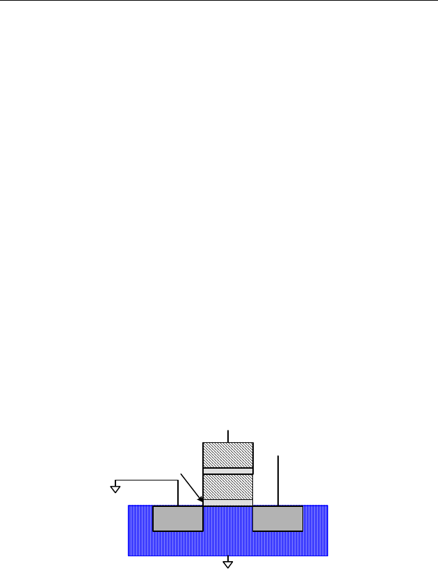
180 SOLUTIONS chapter 5
Sarah L. Harris and David Money Harris, Digital Design and Computer Architecture: ARM® Edition © 2015
by Elsevier Inc. Exercise Solutions
Exercise 5.53
http://www.intel.com/design/flash/articles/what.htm
Flash memory is a nonvolatile memory because it retains its contents after
power is turned off. Flash memory allows the user to electrically program and
erase information. Flash memory uses memory cells similar to an EEPROM,
but with a much thinner, precisely grown oxide between a floating gate and the
substrate (see Figure 5.9).
Flash programming occurs when electrons are placed on the floating gate.
This is done by forcing a large voltage (usually 10 to 12 volts) on the control
gate. Electrons quantum-mechanically tunnel from the source through the thin
oxide onto the control gate. Because the floating gate is completely insulated by
oxide, the charges are trapped on the floating gate during normal operation. If
electrons are stored on the floating gate, it blocks the effect of the control gate.
The electrons on the floating gate can be removed by reversing the procedure,
i.e., by placing a large negative voltage on the control ga
te.
The default state of a flash bitcell (when there are no electrons on the float-
ing gate) is ON, because the channel will conduct when the wordline is HIGH.
After the bitcell is programmed (i.e., when there are electrons on the floating
gate), the state of the bitcell is OFF, because the floating gate blocks the effect
of the control gate. Flash memory is a key element in thumb drives, cell phones,
digital cameras, Blackberries, and other low-power devices that must retain
their memory when turned off.
FIGURE 5.9 Flash EEPROM
n
p
wordline
bitline
substrate
floating
gate
n
GND
control
gate
source
drain
thin
oxide
SOLUTIONS
181
Sarah L. Harris and David Money Harris, Digital Design and Computer Architecture: ARM® Edition © 2015 by Elsevier
Inc. Exercise Solutions
Exercise 5.55
Exercise 5.57
(a) Number of inputs = 2 16 + 1 = 33
Number of outputs = 16 + 1 = 17
Thus, this would require a 2
33
x 17-bit ROM.
(b) Number of inputs = 16
Number of outputs = 16
Thus, this would require a 2
16
x 16-bit ROM.
(c) Number of inputs = 16
Number of outputs = 4
Thus, this would require a 2
16
x 4-bit ROM.
All of these implementations are not good design choices. They could all
be implemented in a smaller amount of hardware using discrete gates.
4:16
Decoder
A,B,C,D
ZYX
4
0000
0010
0100
0110
1000
1010
1100
1110
0001
0011
0101
0111
1001
1011
1101
1111
182 SOLUTIONS chapter 5
Sarah L. Harris and David Money Harris, Digital Design and Computer Architecture: ARM® Edition © 2015
by Elsevier Inc. Exercise Solutions
Exercise 5.59
(a) 1 LE
(b) 2 LEs
LUT output
00
01
10
11
1
1
1
1
data 2
0
0
0
0
00
01
10
11
1
1
1
1
1
1
1
1
data 1
(A)(B)(C)(Y)
data 4data 3
data 1
D
A
B
C
X
data 2
data 3
data 4
LUT
LE
00
01
10
11
0
0
0
0
00
01
10
11
1
1
1
1
0
0
0
0
0
0
0
0
1
1
1
1
1
1
1
1
1
1
1
0
0
1
0
1
(D)
LUT output
00
01
10
11
1
1
1
1
data 2
0
0
0
0
00
01
10
11
1
1
1
1
1
0
0
0
data 1
(B) (C) (D) (X)
data 4data 3
data 1
D
A
B
CX
data 2
data 3
data 4
LUT
LE 1
00
01
10
11
0
0
0
0
00
01
10
11
1
1
1
1
0
0
0
0
0
0
0
0
1
1
1
1
1
1
1
1
1
0
0
0
1
0
0
0
(E)
LUT output
XX
XX
XX
XX
0
1
1
1
data 2
0
data 1
(A) (X) (Y)
data 4data 3
0
data 1A
0 Y
data 2
data 3
data 4
LUT
LE 2
01
10
11
0

SOLUTIONS 183
Sarah L. Harris and David Money Harris, Digital Design and Computer Architecture: ARM® Edition © 2015 by Elsevier
Inc. Exercise Solutions
(c) 2 LEs
LUT output
00
01
10
11
data 2
0
0
0
0
00
01
10
11
1
1
1
1
data 1
(A) (B) (C) (Y)
data 4data 3
data 1
D
A
B
CY
data 2
data 3
data 4
LUT
LE 1
00
01
10
11
0
0
0
0
00
01
10
11
1
1
1
1
0
0
0
0
0
0
0
0
1
1
1
1
1
1
1
1
(D)
LUT output
00
01
10
11
data 2
0
0
0
0
00
01
10
11
1
1
1
1
data 1
(A) (B) (C) (Z)
data 4data 3
00
01
10
11
0
0
0
0
00
01
10
11
1
1
1
1
0
0
0
0
0
0
0
0
1
1
1
1
1
1
1
1
(D)
data 1A
B
CZ
data 2
data 3
data 4
LUT
LE 2
D
0
1
0
1
0
1
0
1
1
1
1
0
1
0
0
1
0
0
0
0
0
1
0
1
1
0
0
0
1
0
1
0
184 SOLUTIONS chapter 5
Sarah L. Harris and David Money Harris, Digital Design and Computer Architecture: ARM® Edition © 2015
by Elsevier Inc. Exercise Solutions
(d) 2 LEs
LUT output
00
01
10
11
data 2
0
0
0
0
00
01
10
11
1
1
1
1
data 1
(A
3
)(D)
data 4data 3
data 1A
3
D
data 2
data 3
data 4
LUT
LE 1
00
01
10
11
0
0
0
0
00
01
10
11
1
1
1
1
0
0
0
0
0
0
0
0
1
1
1
1
1
1
1
1
LUT output
00
01
10
11
data 2
0
0
0
0
00
01
10
11
1
1
1
1
data 1
(P)
data 4data 3
00
01
10
11
0
0
0
0
00
01
10
11
1
1
1
1
0
0
0
0
0
0
0
0
1
1
1
1
1
1
1
1
data 1
P
data 2
data 3
data 4
LUT
LE 2
(A
2
)(A
1
)(A
0
)(A
3
)(A
2
)(A
1
)(A
0
)
A
2
A
1
A
0
A
3
A
2
A
1
A
0
0
0
0
1
0
0
1
0
1
0
0
1
0
0
1
0
0
0
1
1
0
1
0
1
0
0
1
0
1
0
0
0

SOLUTIONS 185
Sarah L. Harris and David Money Harris, Digital Design and Computer Architecture: ARM® Edition © 2015 by Elsevier
Inc. Exercise Solutions
(e) 2 LEs
Exercise 5.61
(a) 5 LEs (2 for next state logic and state registers, 3 for output logic)
(b)
t
pd
= t
pd_LE
+ t
wire
= (381+246) ps
= 627 ps
T
c
t
pcq
+ t
pd
+ t
setup
[199 + 627 + 76] ps
= 902 ps
f = 1 / 902 ps = 1.1 GHz
(c)
First, we check that there is no hold time violation with this amount of clock
skew.
t
cd_LE
= t
pd_LE
= 381 ps
t
cd
= t
cd_LE
+ t
wire
= 627 ps
LUT output
00
01
10
11
data 2
0
0
0
0
00
01
10
11
1
1
1
1
data 1
(A
3
)
data 4data 3
data 1A
3
data 2
data 3
data 4
LUT
LE 1
00
01
10
11
0
0
0
0
00
01
10
11
1
1
1
1
0
0
0
0
0
0
0
0
1
1
1
1
1
1
1
1
LUT output
00
01
10
11
data 2
0
0
0
0
00
01
10
11
1
1
1
1
data 1 data 4data 3
00
01
10
11
0
0
0
0
00
01
10
11
1
1
1
1
0
0
0
0
0
0
0
0
1
1
1
1
1
1
1
1
data 1
data 2
data 3
data 4
LUT
LE 2
(A
2
)(A
1
)(A
0
)(A
3
)(A
2
)(A
1
)(A
0
)
A
2
A
1
A
0
A
3
A
2
A
1
A
0
(Y
0
)(Y
1
)
0
0
1
1
0
0
0
0
1
1
1
1
1
1
1
1
0
0
0
0
1
1
1
1
1
1
1
1
1
1
1
1
Y
0
Y
1

186 SOLUTIONS chapter 5
Sarah L. Harris and David Money Harris, Digital Design and Computer Architecture: ARM® Edition © 2015
by Elsevier Inc. Exercise Solutions
t
skew
< (t
ccq
+ t
cd
) - t
hold
< [(199 + 627) - 0] ps
< 826 ps
3 ns is less than 826 ps, so there is no hold time violation.
Now we find the fastest frequency at which it can run.
T
c
t
pcq
+ t
pd
+ t
setup
+ t
skew
[0.902 + 3] ns
= 3.902 ns
f = 1 / 3.902 ns = 256 MHz
Exercise 5.63
First, we find the cycle time:
T
c
= 1/f = 1/100 MHz = 10 ns
T
c
t
pcq
+ Nt
LE+wire
+ t
setup
10 ns [0.199 + N(0.627) + 0.076] ns
Thus, N <
15.5
The maximum number of LEs on the critical path is 15.
With at most one LE on the critical path and no clock skew, the fastest the
FSM will run is:
T
c
[0.199 + 0.627 + 0.076] ns
0.902 ns
f = 1 / 0.902 ns = 1.1 GHz
Question 5.1
(2
N
-1)(2
N
-1) = 2
2N
- 2
N+1
+1

SOLUTIONS 187
Sarah L. Harris and David Money Harris, Digital Design and Computer Architecture: ARM® Edition © 2015 by Elsevier
Inc. Exercise Solutions
Question 5.3
FIGURE 5.10 BCD adder: (a) 4-bit block, (b) underlying hardware, (c) 8-bit BCD adder
+
4 4
5
-
5
10
0
1
4 4
[3:0]
[4]
[3:0]
4
S
3:0
C
out
C
in
BCD+
4
44
A
3:0
B
3:0
A
3:0
B
3:0
C
in
S
3:0
C
out
(a) (b)
BCD+
4
44
A
7:4
B
7:4
S
7:4
C
out
(c)
BCD+
4
44
A
3:0
B
3:0
C
in
S
3:0
188 SOLUTIONS chapter 5
Sarah L. Harris and David Money Harris, Digital Design and Computer Architecture: ARM® Edition © 2015
by Elsevier Inc. Exercise Solutions
(continued from previous page)
SystemVerilog
module bcdadd_8(input logic [7:0] a, b,
input logic cin,
output logic [7:0] s,
output logic cout);
logic c0;
bcdadd_4 bcd0(a[3:0], b[3:0], cin, s[3:0], c0);
bcdadd_4 bcd1(a[7:4], b[7:4], c0, s[7:4], cout);
endmodule
module bcdadd_4(input logic [3:0] a, b,
input logic cin,
output logic [3:0] s,
output logic cout);
logic [4:0] result, sub10;
assign result = a + b + cin;
assign sub10 = result - 10;
assign cout = ~sub10[4];
assign s = sub10[4] ? result[3:0] : sub10[3:0];
endmodule
VHDL
library IEEE; use IEEE.STD_LOGIC_1164.all;
entity bcdadd_8 is
port(a, b: in STD_LOGIC_VECTOR(7 downto 0);
cin: in STD_LOGIC;
s: out STD_LOGIC_VECTOR(7 downto 0);
cout: out STD_LOGIC);
end;
architecture synth of bcdadd_8 is
component bcdadd_4
port(a, b: in STD_LOGIC_VECTOR(3 downto 0);
cin: in STD_LOGIC;
s: out STD_LOGIC_VECTOR(3 downto 0);
cout: out STD_LOGIC);
end component;
signal c0: STD_LOGIC;
begin
bcd0: bcdadd_4
port map(a(3 downto 0), b(3 downto 0), cin, s(3
downto 0), c0);
bcd1: bcdadd_4
port map(a(7 downto 4), b(7 downto 4), c0, s(7
downto 4), cout);
end;
library IEEE; use IEEE.STD_LOGIC_1164.all;
use IEEE.STD_LOGIC_UNSIGNED.all;
use IEEE.STD_LOGIC_ARITH.all;
entity bcdadd_4 is
port(a, b: in STD_LOGIC_VECTOR(3 downto 0);
cin: in STD_LOGIC;
s: out STD_LOGIC_VECTOR(3 downto 0);
cout: out STD_LOGIC);
end;
architecture synth of bcdadd_4 is
signal result, sub10, a5, b5: STD_LOGIC_VECTOR(4
downto 0);
begin
a5 <= '0' & a;
b5 <= '0' & b;
result <= a5 + b5 + cin;
sub10 <= result - "01010";
cout <= not (sub10(4));
s <= result(3 downto 0) when sub10(4) = '1'
else sub10(3 downto 0);
end;

189 SOLUTIONS chapter 6 S. Harris and D.M. Harris, DDCA: ARM® Edition © 2015 Elsevier, Inc.
CHAPTER 6
E
xercise 6.1
(1) Regularity supports simplicity
• Each instruction has a 2-bit opcode.
• Each instruction has a 4-bit condition code.
• ARM has 3 instruction formats for the most common instructions (Data-processing
format, Memory format, and Branch format).
• The Data-processing and Memory instruction formats have a similar number and
order of operands.
• Each instruction is the same size, making decoding hardware simple.
(2) Make the common case fast
• Registers make the access to most recently accessed variables fast.
• The RISC (reduced instruction set computer) architecture, makes the common/simple
instructions fast because the computer must handle only a small number of simple
instructions.
• Most instructions require all 32 bits of an instruction, so all instructions are 32 bits
(even though some would have an advantage of a larger instruction size and others a
smaller instruction size). The instruction size is chosen to make the common
instructions fast.
(3) Smaller is faster
• The register file has only 16 registers.
• The ISA (instruction set architecture) includes only a small number of commonly
used instructions. This keeps the hardware small and, thus, fast.
• The instruction size is kept small to make instruction fetch fast.
(4) Good design demands good compromises
• ARM uses three instruction formats (instead of just one).
• Ideally all accesses would be as fast as a register access, but ARM architecture also
supports main memory accesses to allow for a compromise between fast access time
and a large amount of memory.
• Because ARM is a RISC architecture, it includes only a set of simple instructions, but
it provides pseudocode to the user and compiler for commonly used operations, like
NOP.
• ARM provides three formats to encode immediate values (and four if you count the 5-
bit immediate encoding for a shift, shamt5):
{
rot
3:0
, imm8
7:0
} for data-processing instructions
imm12
11:0
for memory instructions

190 SOLUTIONS chapter 6 S. Harris and D.M. Harris, DDCA: ARM® Edition © 2015 Elsevier, Inc.
imm24
23:0
for branch instructions
Exercise 6.3
(a) 42 × 4 = 42 × 22 = 1010102 << 2 = 101010002 = 0xA8
(b) 0xA8 through 0xAB
(c)
Exercise 6.5
In big-endian format, the bytes are numbered from 100 to 103 from left to right. In little-endian
format, the bytes are numbered from 100 to 103 from right to left. Thus, the load byte instruction
(LDRB) returns a different value depending on the endianness of the machine. At the end of the
program R2 contains 0xBC on a big-endian machine and 0xD8 on a little-endian machine.
Exercise 6.7
(a) 0x68 6F 77 64 79 00
(b) 0x6C 69 6F 6E 73 00
(c) 0x54 6F 20 74 68 65 20 72 65 73 63 75 65 21 00

191
SOLUTIONS chapter 6 S. Harris and D.M. Harris, DDCA: ARM® Edition © 2015 Elsevier, Inc.
Exercise 6.9
Exercise 6.11
0xE0808001
0xE593B004
0xE2475058
0xE1A03702
Exercise 6.13
(a) SUB R5, R7, #0x58
(b) rot = 0, imm8 = 0x58
Exercise 6.15
ARM Assembly
; R0 = decimal number, R1 = base address of array,
; R2 = val, R3 = tmp
MOV R2, #31
L1 LSR R3, R0, R2
AND R3, R3, #1
STRB R3, [R1], #1
SUBS R2, R2, #1

192 SOLUTIONS chapter 6 S. Harris and D.M. Harris, DDCA: ARM® Edition © 2015 Elsevier, Inc.
BPL L1
L2 MOV PC, LR
C Code
void convert2bin(int num, char binarray[]){
int i;
char tmp, val = 31;
for (i=0; i<32; i++) {
tmp = (num >> val) & 1;
binarray[i] = tmp;
val--;
}
}
In words
This program converts an unsigned integer (R0) from decimal to binary and stores it in an array
pointed to by R1.
Exercise 6.17
AND R0, R1, R2
MVN R0, R0
Exercise 6.19
(a)
(i)
CMP R0, R1 ; g > h?
BLE ELSE
ADD R0, R0, #1 ; g = g + 1
B DONE
ELSE SUB R0, R1, #1 ; g = h - 1
DONE
(ii)
CMP R0, R1 ; g <= h?
BGT ELSE
MOV R0, #0 ; g = 0
B DONE
ELSE MOV R1, #0 ; h = 0
DONE

193
SOLUTIONS chapter 6 S. Harris and D.M. Harris, DDCA: ARM® Edition © 2015 Elsevier, Inc.
(b)
(i)
CMP R0, R1 ; g > h?
ADDGT R0, R0, #1 ; g = g + 1
SUBLE R1, R1, #1 ; h = h – 1
(ii)
CMP R0, R1 ; g <= h?
MOVLE R0, #1 ; g = 0
MOVGT R1, #0 ; h = 0
(c) When conditional execution is available for all instructions, it takes 3 instructions,
compared to 5 instructions when conditional execution is allowed only for branch instructions.
So, in this case, allowing conditional execution for all instructions results in a 40% decrease in
the number of instructions.
Thus, the advantages of conditional execution are (1) 40% less memory required for instruction
storage, and (2) potentially decreased execution time. The execution time of the code in part (a)
is 3-4 instructions, whereas it is 3 instructions in part (b). As will be seen in Chapter 7, the
number of instructions fetched in part (a) can be even higher when using a pipelined processor.
A disadvantage of (b) over (a) is that all instructions require a condition code, which uses four
bits of encoding that could be used for something else. However, as shown, this cost in bits used
for encoding the condition is usually well worth it.
Exercise 6.21
(a)
ADD R2, R3, #0x190 ; R2 = end of array
FOR CMP R3, R2 ; reached end of array?
BGE DONE
LDR R1, [R3] ; R1 = array[i]
LSL R1, R1, #5 ; R1 = array[i] * 32
STR R1, [R3] ; array[i] = array[i] * 32
ADD R3, R3, #4 ; R3 points to next array entry
B FOR
DONE
(b)
ADD R2, R3, #0x190 ; R2 = end of array

194
SOLUTIONS chapter 6 S. Harris and D.M. Harris, DDCA: ARM® Edition © 2015 Elsevier, Inc.
FOR CMP R3, R2 ; reached end of array?
BGE DONE
LDR R1, [R3] ; R1 = array[i]
LSL R1, R1, #7 ; R1 = array[i] * 128
STR R1, [R3], #4 ; array[i] = array[i] * 128
; R3 points to next array entry
B FOR
DONE
(c) part (a) has 8 instructions and part (b) has 7 instructions. The loop code particularly decreases
from 7 instructions to 6 instructions. This is a 12.5% decrease in the number of instructions and a
14% decrease in loop instructions. The advantages are: (1) 12.5% lower memory requirements
for code storage, and (2) decreased execution time (approximately 14% decrease because most of
the execution time is spent in the loop). The disadvantage is the number of bits required for
encoding the indexing mode.
Exercise 6.23
(a) Yes.
(b)
(i)
MOV R1, #0 ; i = 0
FOR CMP R1, #10 ; reached end of array?
BGE DONE
LDR R2, [R0, R1, LSL #2] ; R2 = nums[i]
LSR R2, R2, #1 ; R2 = nums[i]/2
STR R2, [R0, R1, LSL #2] ; nums[i] = nums[i]/2
ADD R1, R1, #1 ; i = i + 1
B FOR
DONE
(ii)
MOV R1, #9 ; i = 9
FOR LDR R2, [R0, R1, LSL #2] ; R2 = nums[i]
LSR R2, R2, #1 ; R2 = nums[i]/2
STR R2, [R0, R1, LSL #2] ; nums[i] = nums[i]/2
SUBS R1, R1, #1 ; i = i – 1 and set flags
BPL FOR
(c) The second code snippet (ii), the decremented loop, uses fewer instructions and is faster.
Each loop iteration in code snippet (ii) requires 5 instead of the 7 instructions required for code

195
SOLUTIONS chapter 6 S. Harris and D.M. Harris, DDCA: ARM® Edition © 2015 Elsevier, Inc.
snippet (i). Code snippet ii combines checking the loop condition with updating the loop
variable, i.
Exercise 6.25
(a)
; ARM assembly code
; base address of array dst = R0
; base address of array src = R1
; i = R4
STRCPY
PUSH {R4} ; save R4 on stack
MOV R4, #0 ; i = 0
LOOP
LDRB R2, [R1, R4] ; R2 = src[i]
STRB R2, [R0, R4] ; dst[i] = src[i]
CMP R2, #0 ; array[i] == 0? (end of string?)
ADD R4, R4, #1 ; i++
BNE LOOP ; if not, repeat
DONE
POP {R4} ; restore R4
MOV PC, LR ; return
(b) The stack (i) before, (ii) during, and (iii) after the strcpy procedure.
Exercise 6.27
(a)
func1: 8 words (for R4-R10 and LR)
func2: 3 words (for R4-R5 and LR)
func3: 4 words (for R7-R9 and LR)
func4: 1 word (for R11)
(b)

196 SOLUTIONS chapter 6 S. Harris and D.M. Harris, DDCA: ARM® Edition © 2015 Elsevier, Inc.
Exercise 6.29
(a) 120
(b) (2)
(c) (i) (3) returned value is R1
4
(ii) (3) returned value is R1
4
(iii) (4)
Exercise 6.31
(a) 0xa0000001
(b) 0xaa00000e
(c) 0x8afff841
(d) 0xeb00391d
(e) 0xeaffe3fc

197
SOLUTIONS chapter 6 S. Harris and D.M. Harris, DDCA: ARM® Edition © 2015 Elsevier, Inc.
Exercise 6.33
(a)
; R4 = i, R5 = num
SETARRAY
PUSH {R4, R5, LR} ; save R4, R5, and LR on the stack
SUB SP, SP, #40 ; allocate space on stack for array
MOV R4, #0 ; i = 0
MOV R5, R0 ; R5 = num
LOOP MOV R1, R4 ; set up input arguments
BL COMPARE ; call compare function
STR R0, [SP, R4, LSL #2] ; array[i] = return value
ADD R4, R4, #1 ; increment i
MOV R0, R5 ; arg0 = num
CMP R4, #10 ; i < 10?
BLT LOOP
ADD SP, SP, #40 ; deallocate space on stack for array
POP {R4, R5, LR} ; restore registers
MOV PC, LR ; return to point of call
COMPARE
PUSH {LR} ; save LR
BL SUBFUNC ; call sub function
CMP R0, #0 ; returned value >= 0?
MOVGE R0, #1 ; if yes, R0 = 1
MOVLT R0, #0 ; if no, R0 = 0
POP {LR} ; restore LR
MOV PC, LR ; return to point of call
SUBFUNC
SUB R0, R0, R1 ; return a-b
MOV PC, LR ; return to point of call
(b)

198
SOLUTIONS chapter 6 S. Harris and D.M. Harris, DDCA: ARM® Edition © 2015 Elsevier, Inc.
(c) The code would enter an infinite loop and eventually crash. When the compare function
returns (MOV PC, LR), instead of returning to its point of call in the setArray function, the
compare function would continue executing at the instruction just after the call to sub (BL
SUBFUNC). Because of the POP {LR} instruction, the program would eventually crash when it
went beyond the stack space available (i.e., the stack pointer was decremented past the allocated
dynamic data segment).

199
SOLUTIONS chapter 6 S. Harris and D.M. Harris, DDCA: ARM® Edition © 2015 Elsevier, Inc.
Exercise 6.35
The largest address offset (imm24) a branch instruction (B or BL) can encode is 2
24
-1 =
16,777,215. Since the offset adds to the address 2 instructions ahead of the current instruction
(i.e., at PC + 8), a branch can branch forward at most (2
24
-1) + 2 = 16,777,217 instructions.
Because instructions are relative to PC + 4, it can branch forward between 0 and 16,777,217
instructions relative to the current instruction. So, if the current instruction address is 0x0. The
farthest it can branch forward is to instruction address 16,777,217 * 4 = 67,108,868 =
0x4000004.
Exercise 6.37
It is advantageous to have a large address field in the machine format for branch instructions to
increase the range of instruction addresses to which the instruction can branch.
Exercise 6.39
// High-Level Code
void little2big(int[] array) {
int i;
for (i = 0; i < 10; i = i + 1) {
array[i] = ((array[i] << 24) |
((array[i] & 0xFF00) << 8) |
((array[i] & 0xFF0000) >> 8) |
((array[i] >> 24) & 0xFF));
}
}
; ARM Assembly Code
; R0 = base address of array, R12 = i
little2BIG
MOV R12, #0 ; i = 0
LOOP
CMP R12, #10 ; i < 10?
BGE DONE
LDR R2, [R0, R12, LSL #2] ; R2 = array[i]
LSL R3, R2, #24 ; R3 = array[i] << 24
AND R4, R2, #0xFF00 ; R4 = (array[i] & 0xFF00)
ORR R3, R3, R4, LSL #8 ; R3 = top two bytes
AND R4, R2, #0xFF0000 ; R4 = (array[i] & 0xFF0000)
ORR R3, R3, R4, LSR #8 ; R3 = top three bytes
ORR R3, R3, R2, LSR #24 ; R3 = all four bytes
STR R3, [R0, R12, LSL #2] ; array[i] = R3
ADD R12, R12, #1 ; increment i
B LOOP
DONE
MOV PC, LR

200 SOLUTIONS chapter 6 S. Harris and D.M. Harris, DDCA: ARM® Edition © 2015 Elsevier, Inc.
Exercise 6.41
; R4, R5 = mantissas of a, b, R6, R7 = exponents of a, b
FLPADD
PUSH {R4, R5, R6, R7, R8} ; save registers that will be used
LDR R2, =0x007fffff ; load mantissa mask
LDR R3, =0x7f800000 ; load exponent mask
AND R4, R0, R2 ; extract mantissa from R0 (a)
AND R5, R1, R2 ; extract mantissa from R1 (b)
ORR R4, R4, #0x800000 ; insert implicit leading 1
ORR R5, R5, #0x800000 ; insert implicit leading 1
AND R6, R0, R3 ; extract exponent from R0 (a)
LSR R6, R6, #23 ; shift exponent right
AND R7, R1, R3 ; extract exponent from R1 (b)
LSR R7, R7, #23 ; shift exponent right
MATCH
CMP R6, R7 ; compare exponents
BEQ ADDMANTISSA ; if equal, skip to adding mantissas
BHI SHIFTB ; if a's exponent is bigger, shift b
SHIFTA
SUB R8, R7, R6 ; R8 = b's exponent – a's exponent
ASR R4, R4, R8 ; right-shift a's mantissa
ADD R6, R6, R8 ; update a's exponent
B ADDMANTISSA ; now add the mantissas
SHIFTB
SUB R8, R6, R7 ; R8 = a's exponent – b's exponent
ASR R5, R5, R8 ; right-shift b's mantissa
ADDMANTISSA
ADD R4, R4, R5 ; R4 = sum of mantissas
NORMALIZE
ANDS R5, R4, #0x1000000 ; extract overflow bit
BEQ DONE ; branch to DONE if bit 24 == 0
LSR R4, R4, #1 ; right-shift mantissa by 1 bit
ADD R6, R6, #1 ; increment exponent
DONE
AND R4, R4, R2 ; mask fraction
LSL R6, R6, #23 ; shift exponent into place
ORR R0, R4, R6 ; combine mantissa and exponent
POP {R4, R5, R6, R7, R8} ; restore registers
MOV PC, LR ; return to caller

201 SOLUTIONS chapter 6 S. Harris and D.M. Harris, DDCA: ARM® Edition © 2015 Elsevier, Inc.
Exercise 6.43
(a)
; ARM assembly code
0x8534 MAIN PUSH {R4,LR}
0x8538 MOV R4, #15
0x853c LDR R3, =L2
0x8540 STR R4, [R3]
0x8544 MOV R1, #27
0x8548 STR R1, [R3, #4]
0x854c LDR R0, [R3]
0x8550 BL GREATER
0x8554 POP {R4,LR}
0x8558 MOV PC, LR
0x855c GREATER CMP R0, R1
0x8560 MOV R0, #0
0x8564 MOVGT R0, #1
0x8568 MOV PC, LR
...
0x9305 L2
(b)
Symbol Table
Address Label
0x8534 MAIN
0x8550 GREATER
0x9305 L2
(c)
; machine code ;address ARM assembly
E92D4010 ;0x8534 MAIN PUSH {R4,LR}
; STMDB R13!,{R4,R14}
E3A0400F ;0x8538 MOV R4, #15
E59F3DC1 ;0x853c LDR R3, =L2
E5834000 ;0x8540 STR R4, [R3]
E3A0101B ;0x8544 MOV R1, #27
E5831004 ;0x8548 STR R1, [R3, #4]
E5930000 ;0x854c LDR R0, [R3]
EB000001 ;0x8550 BL GREATER
E8BD4010 ;0x8554 POP {R4,LR}
; LDMIA R13!,{R4,R14}
E1A0F00E ;0x8558 MOV PC, LR
E1500001 ;0x855c GREATER CMP R0, R1
E3A00000 ;0x8560 MOV R0, #0
C3A00001 ;0x8564 MOVGT R0, #1
E1A0F00E ;0x8568 MOV PC, LR
...

202 SOLUTIONS chapter 6 S. Harris and D.M. Harris, DDCA: ARM® Edition © 2015 Elsevier, Inc.
;0x9305 L2
(d)
Text Segment: 15*4 = 60 bytes
Data segment: 4 bytes
Exercise 6.45
Advantages of conditional execution:
• Potentially decreased code size (increased code density)
• Potentially decreased execution time (improved performance)
Disadvantages:
• More complex hardware required to implement it
• Requires 4 instruction bits to encode
Question 6.1
EOR R0, R0, R1 ; R0 = R0 XOR R1
EOR R1, R0, R1 ; R1 = original value of R0
EOR R0, R0, R1 ; R0 = original value of R1
Question 6.3
C Code
void reversewords(char[] array) {
int i, j, length;
// find length of string
for (i = 0; array[i] != 0; i = i + 1)
;
length = i;
// reverse characters in string
reverse(array, length-1, 0);
// reverse words in string
i = 0; j = 0;
// check for spaces or end of string
while (i <= length) {
if ( (i != length) && (array[i] != 0x20) ) {
i = i + 1;
}
else {
203
SOLUTIONS chapter 6 S. Harris and D.M. Harris, DDCA: ARM® Edition © 2015 Elsevier, Inc.
reverse(array, i-1, j);
i = i + 1; // j and i at start of next word
j = i;
}
}
}
void reverse(char[] array, int i, int j) {
char tmp;
while (i > j) {
tmp = array[i];
array[i] = array[j];
array[j] = tmp;
i = i-1;
j = j+1;
}
}
ARM Assembly
; R4 = i, R5 = j, R6 = length
REVERSEWORDS
PUSH {R4,R5,R6} ; save registers on stack
MOV R4, #0 ; i = 0
GETLENGTH
LDRB R1, [R0, R4] ; R1 = array[i]
CMP R1, #0 ; end of string?
ADDNE R4, R4, #1 ; i = i + 1
BNE GETLENGTH
STRINGREVERSE
MOV R6, R4 ; length = i
SUB R1, R6, #1 ; arg1 = length-1
MOV R2, #0 ; arg2 = 0
BL REVERSE ; call reverse function
MOV R4, #0 ; i = 0
MOV R5, #0 ; j = 0
WHILE19
CMP R4, R6 ; i <= length?
BGT DONE19 ; if at end of string, return
BEQ ELSE19 ; if (i == length), do else block
LDRB R1, [R0, R4] ; R1 = array[i]
CMP R1, #0x20 ; array[i] != 0x20?
BEQ ELSE19 ; if (array[i] == 0x20), do else block
ADD R4, R4, #1
B WHILE19 ; repeat while loop
ELSE19
SUB R1, R4, #1 ; arg1 = i-1
MOV R2, R5 ; arg2 = j
BL REVERSE ; call reverse function
ADD R4, R4, #1 ; i = i+1

204 SOLUTIONS chapter 6 S. Harris and D.M. Harris, DDCA: ARM® Edition © 2015 Elsevier, Inc.
MOV R5, R4 ; j = i
B WHILE19 ; repeat while loop
DONE19
POP {R4,R5,R6} ; restore registers from stack
MOV PC, LR ; retrn to calling function
REVERSE
CMP R1, R2 ; i > j?
BLE RETURN19
LDRB R3, [R0, R1] ; R3 = array[i]
LDRB R12, [R0, R2] ; R12 = array[j]
STRB R12, [R0, R1] ; array[i] = array[j]
STRB R3, [R0, R2] ; array[j] = tmp
SUB R1, R1, #1 ; i = i – 1
ADD R2, R2, #1 ; j = j + 1
B REVERSE ; continue while loop
RETURN19
MOV PC, LR
Qu
estion 6.5
C Code
num = swap(num, 1, 0x55555555); // swap bits
num = swap(num, 2, 0x33333333); // swap pairs
num = swap(num, 4, 0x0F0F0F0F); // swap nibbles
num = swap(num, 8, 0x00FF00FF); // swap bytes
num = swap(num, 16, 0xFFFFFFFF); // swap halves
// swap function swaps masked bits
int swap(int num, int shamt, unsigned int mask) {
return ((num >> shamt) & mask) | ((num & mask) << shamt);
AR
M Assembly Code
MOV R0, R3 ; arg0 = num
MOV R1, #1 ; arg1 = 1
LDR R2, =0x55555555 ; arg2 = 0x55555555
BL SWAP ; call swap function
MOV R1, #2 ; arg1 = 1
LDR R2, =0x33333333 ; arg2 = 0x33333333
BL SWAP ; call swap function
MOV R1, #4 ; arg1 = 1
LDR R2, =0x0F0F0F0F ; arg2 = 0x0F0F0F0F
BL SWAP ; call swap function
MOV R1, #8 ; arg1 = 1
LDR R2, =0x00FF00FF ; arg2 = 0x00FF00FF
BL SWAP ; call swap function

205 SOLUTIONS chapter 6 S. Harris and D.M. Harris, DDCA: ARM® Edition © 2015 Elsevier, Inc.
MOV R1, #16 ; arg1 = 1
LDR R2, =0xFFFFFFFF ; arg2 = 0xFFFFFFFF
BL SWAP ; call swap function
MOV R3, R0 ; num = returned value
...
SWAP
LSR R3, R0, R1 ; R3 = num >> shamt
AND R3, R3, R2 ; R3 = (num >> shamt) & mask
AND R0, R0, R2 ; R0 = num & mask
LSL R0, R0, R1 ; R0 = (num & mask) << shamt
ORR R0, R3, R0 ; return val = R3 | R0
MOV PC, LR ; return to caller
Question 6.7
C Code
bool palindrome(char* array) {
int i, j; // array indices
// find length of string
for (j = 0; array[j] != 0; j=j+1) ;
j = j-1; // j is index of last char
i = 0;
while (j > i) {
if (array[i] != array[j])
return false;
j = j-1;
i = i+1;
}
return true;
}
MIPS Assembly Code
; R1 = i, R2 = j, R0 = base address of string
PALINDROME
PUSH {R4} ; save R4 on stack
MOV R2, #0 ; j = 0
GETLENGTH
LDRB R3, [R0, R2] ; R3 = array[j]
CMP R3, #0 ; end of string?
ADDNE R2, R2, #1 ; j = j + 1
BNE GETLENGTH
SUB R2, R2, #1 ; j = j – 1
MOV R1, #0 ; i = 0
WHILE
CMP R2, R1 ; j > i?
BLE RETURNTRUE
LDRB R3, [R0, R1] ; R3 = array[i]
206 SOLUTIONS chapter 6 S. Harris and D.M. Harris, DDCA: ARM® Edition © 2015 Elsevier, Inc.
LDRB R4, [R0, R2] ; R4 = array[j]
CMP R3, R4 ; array[i] == array[j]?
BNE RETURNFALSE
SUB R2, R2, #1 ; j = j-1
ADD R1, R1, #1 ; i = i+1
B WHILE
RETURNTRUE
MOV R0, #1 ; return TRUE
B DONE
RETURNFALSE
MOV R0, #0 ; return FALSE
DONE
POP {R4} ; restore R4
MOV PC, LR ; return to caller

207 SOLUTIONS chapter 7 S. Harris and D.M. Harris, DDCA: ARM® Edition © 2015 Elsevier, Inc.
CHAPTER 7
E
xercise 7.1
(a) ADD, SUB, AND, ORR, LDR: the result never gets written to the register file.
(b) SUB, AND, ORR: the ALU only performs addition
(c) STR: the data memory never gets written
Exercise 7.3
(a) TST
ALU Decoder truth table
ALUOp
Funct
4:1
(
cmd
)
Funct
0
(
S
)
Notes
ALUControl
1:0
FlagW
1:0
NoWrite
0
X
X
Not DP
00
00
0
1
0100
0 ADD
00
00
0
1
11
0
0010
0 SUB
01
00
0
1
11
0
0000
0 AND
10
00
0
1
10
0
1100
0 ORR
11
00
0
1
10
0
1000
1
TST
10
10
1
Control Unit Schematic

208
SOLUTIONS chapter 7 S. Harris and D.M. Harris, DDCA: ARM® Edition © 2015 Elsevier, Inc.
Conditional
Logic
Condition
Check
CondEx
(b) LSL
Single-cycle datapath
+
Instr
ALU
+
RegSrc

209
SOLUTIONS chapter 7 S. Harris and D.M. Harris, DDCA: ARM® Edition © 2015 Elsevier, Inc.
Control unit
ALU Decoder truth table
ALUOp
Funct
4:1
(
cmd
)
Funct
0
(
S
)
Notes
ALUControl
1:0
FlagW
1:0
Shift
0
X
X
Not DP
00
00
0
1
0100
0 ADD
00
00
0
1
11
0
0010
0 SUB
01
00
0
1
11
0
0000
0 AND
10
00
0
1
10
0
1100
0 ORR
11
00
0
1
10
0
1101
0 LSL
XX
00
1
1
10
1

210
SOLUTIONS chapter 7 S. Harris and D.M. Harris, DDCA: ARM® Edition © 2015 Elsevier, Inc.
(c) CMN
ALU Decoder truth table
ALUOp
Funct
4:1
(
cmd
)
Funct
0
(
S
)
Notes
ALUControl
1:0
FlagW
1:0
NoWrite
0
X
X
Not DP
00
00
0
1
0100
0 ADD
00
00
0
1
11
0
0010
0 SUB
01
00
0
1
11
0
0000
0 AND
10
00
0
1
10
0
1100
0 ORR
11
00
0
1
10
0
1011
1
CMN
00
11
1
Control Unit schematic

211
SOLUTIONS chapter 7 S. Harris and D.M. Harris, DDCA: ARM® Edition © 2015 Elsevier, Inc.
ImmSrc
1:0
MemW
MemtoReg
ALUSrc
ALUControl
1:0
Decoder
RegW
Cond
3:0
Op
1:0
Funct
5:0
Rd
3:0
RegSrc
1:0
FlagW
1:0
ALUFlags
3:0
MemWrite
RegWrite
PCSrc
PCS
Main
Decoder
ALUOp
ALU
Decoder
Op
1:0
Funct
5:0
Rd
3:0
5,0
PC Logic PCS
FlagW
1:0
ALUControl
1:0
Branch
ImmSrc
1:0
MemtoReg
ALUSrc
RegSrc
1:0
MemW
RegW
Cond
3:0
Flags
3:2
CLK
CLK
ALUFlags
3:0
Flags
1:0
[3:2]
[1:0]
FlagWrite
1:0
[1]
[0]
FlagW
1:0
PCSrc
MemWrite
RegWrite
PCS
MemW
RegW
(c) Conditional Logic
4:0
CLK
(a) Control Unit
Decoder(b)
NoWrite
NoWrite
NoWrite
(d) ADC
ALU Decoder truth table
ALUOp
Funct
4:1
(
cmd
)
Funct
0
(
S
)
Notes
ALUControl
2:0
FlagW
1:0
0
X
X
Not DP
0
00
00
1
0100
0 ADD
0
00
00
1
11
0010
0 SUB
0
01
00
1
11
0000
0 AND
0
10
00
1
10
1100
0 ORR
0
11
00
1
10

212
SOLUTIONS chapter 7 S. Harris and D.M. Harris, DDCA: ARM® Edition © 2015 Elsevier, Inc.
0101
0
ADC
1
00
00
1
11
Single-cycle ARM processor ALU
Single-cycle ARM processor datapath

213
SOLUTIONS chapter 7 S. Harris and D.M. Harris, DDCA: ARM® Edition © 2015 Elsevier, Inc.
Single-cycle ARM processor control unit
Conditional
Logic
Condition
Check
CondEx
Exercise 7.5
It is not possible to implement this instruction without either modifying the register file or
making the instruction take at least two cycles to execute. We modify the register file and
datapath as shown below.
• Add WE1 and WD1 signals to the register file.
• WE1 connects to the PostIndex signal (from control unit)
• WD1 connects to ALUResult, which is the sum of Rn + Rm (or Rn + Src2, more generally).
• Add multiplexer before Data Memory Address to choose between (Rn + Src2) and Rn.
With post-indexing, the Data Memory Address input connects to Rn.

214
SOLUTIONS chapter 7 S. Harris and D.M. Harris, DDCA: ARM® Edition © 2015 Elsevier, Inc.
ExtImm
CLK
A RD
Instruction
Memory
4
A1
A3
WD3
RD2
RD1
WE3
A2
CLK
Register
File
0
1
A RD
Data
Memory
WD
WE
1
0
PC
1
0
PC'
19:16
15:12
23:0
25:20
SrcB
ALUResult
ReadData
WriteData
SrcA
PCPlus4
Result
27:26
ImmSrc
PCSrc
MemWrite
MemtoReg
ALUSrc
RegWrite
Op
Funct
Control
Unit
ALUFlags
CLK
ALUControl
PCPlus8
R15
3:0
Cond
31:28
Flags
15:12
Rd
4
15
RA1
RA2
0 1
Extend
0
1
0
1
WD1
WE1
1
0
PostIndex
PostIndex
PostIndex
We modified the Main Decoder truth table as shown below.
Op
Funct
5:0
Type
Branch
MemtoReg
MemW
ALUSrc
ImmSrc
RegW
RegSrc
ALUOp
PostIndex
00 0XXXXX
DP Reg 0 0 0 0 XX 1 00 1 0
00 1XXXXX
DP Imm 0 0 0 1 00 1 X0 1 0
01 X00000
STR 0 X 1 1 01 0 10 0 0
01 011001
LDR
(offset
indexing,
immediate
offset)
0 1 0 1 01 1 X0 0 0
01 111001
LDR
(offset
indexing,
register
offset)
0 1 0 0 01 1 00 0 0
01 001001
LDR
(post-
indexing,
immediate
offset)
0 1 0 1 01 1 X0 0 1
01 101001
LDR 0 1 0 0 01 1 00 0 1

215
SOLUTIONS chapter 7 S. Harris and D.M. Harris, DDCA: ARM® Edition © 2015 Elsevier, Inc.
(post-
indexing,
register
offset)
Exercise 7.7
She should work on the memory. t
mem
= (200/2) ps = 100 ps
From Equation 7.3, the new cycle time is:
T
c1
= 40 + 2(100) + 70 + 100 + 120 + 2(25) + 60 = 640 ps
Exercise 7.9
SystemVerilog
// ex7.9 solutions
//
// single-cycle ARM processor
// additional instructions: TST, LSL, CMN, ADC
module testbench();
logic clk;
logic reset;
logic [31:0] WriteData, DataAdr;
logic MemWrite;
// instantiate device to be tested
top dut(clk, reset, WriteData, DataAdr, MemWrite);
// initialize test
initial
begin
reset <= 1; # 22; reset <= 0;
end
// generate clock to sequence tests
always
begin
clk <= 1; # 5; clk <= 0; # 5;
end
// check results
always @(negedge clk)
begin
if(MemWrite) begin
if(DataAdr === 20 & WriteData === 2) begin
$display("Simulation succeeded");
$stop;
216
SOLUTIONS chapter 7 S. Harris and D.M. Harris, DDCA: ARM® Edition © 2015 Elsevier, Inc.
end else begin
$display("Simulation failed");
$stop;
end
end
end
endmodule
module top(input logic clk, reset,
output logic [31:0] WriteData, DataAdr,
output logic MemWrite);
logic [31:0] PC, Instr, ReadData;
// instantiate processor and memories
arm arm(clk, reset, PC, Instr, MemWrite, DataAdr,
WriteData, ReadData);
imem imem(PC, Instr);
dmem dmem(clk, MemWrite, DataAdr, WriteData, ReadData);
endmodule
module dmem(input logic clk, we,
input logic [31:0] a, wd,
output logic [31:0] rd);
logic [31:0] RAM[63:0];
assign rd = RAM[a[31:2]]; // word aligned
always_ff @(posedge clk)
if (we) RAM[a[31:2]] <= wd;
endmodule
module imem(input logic [31:0] a,
output logic [31:0] rd);
logic [31:0] RAM[63:0];
initial
$readmemh("ex7.9_memfile.dat",RAM);
assign rd = RAM[a[31:2]]; // word aligned
endmodule
module arm(input logic clk, reset,
output logic [31:0] PC,
input logic [31:0] Instr,
output logic MemWrite,
output logic [31:0] ALUResult, WriteData,
input logic [31:0] ReadData);
logic [3:0] ALUFlags;
logic RegWrite,
ALUSrc, MemtoReg, PCSrc;
217
SOLUTIONS chapter 7 S. Harris and D.M. Harris, DDCA: ARM® Edition © 2015 Elsevier, Inc.
logic [1:0] RegSrc, ImmSrc;
logic [2:0] ALUControl; // ADC
logic carry; // ADC
logic Shift; // LSL
controller c(clk, reset, Instr[31:12], ALUFlags,
RegSrc, RegWrite, ImmSrc,
ALUSrc, ALUControl,
MemWrite, MemtoReg, PCSrc,
carry, // ADC
Shift); // LSL
datapath dp(clk, reset,
RegSrc, RegWrite, ImmSrc,
ALUSrc, ALUControl,
MemtoReg, PCSrc,
ALUFlags, PC, Instr,
ALUResult, WriteData, ReadData,
carry, // ADC
Shift); // LSL
endmodule
module controller(input logic clk, reset,
input logic [31:12] Instr,
input logic [3:0] ALUFlags,
output logic [1:0] RegSrc,
output logic RegWrite,
output logic [1:0] ImmSrc,
output logic ALUSrc,
output logic [2:0] ALUControl, // ADC
output logic MemWrite, MemtoReg,
output logic PCSrc,
output logic carry, // ADC
output logic Shift); // LSL
logic [1:0] FlagW;
logic PCS, RegW, MemW;
logic NoWrite; // TST, CMN
decoder dec(Instr[27:26], Instr[25:20], Instr[15:12],
FlagW, PCS, RegW, MemW,
MemtoReg, ALUSrc, ImmSrc, RegSrc, ALUControl,
NoWrite, // TST, CMN
Shift); // LSL
condlogic cl(clk, reset, Instr[31:28], ALUFlags,
FlagW, PCS, RegW, MemW,
PCSrc, RegWrite, MemWrite,
carry, // ADC
NoWrite); // TST, CMN
endmodule
module decoder(input logic [1:0] Op,
input logic [5:0] Funct,
input logic [3:0] Rd,
output logic [1:0] FlagW,
218 SOLUTIONS chapter 7 S. Harris and D.M. Harris, DDCA: ARM® Edition © 2015 Elsevier, Inc.
output logic PCS, RegW, MemW,
output logic MemtoReg, ALUSrc,
output logic [1:0] ImmSrc, RegSrc,
output logic [2:0] ALUControl, // ADC
output logic NoWrite, // TST, CMN
output logic Shift); // LSL
logic [9:0] controls;
logic Branch, ALUOp;
// Main Decoder
always_comb
case(Op)
// Data processing immediate
2'b00: if (Funct[5]) controls = 10'b0000101001;
// Data processing register
else controls = 10'b0000001001;
// LDR
2'b01: if (Funct[0]) controls = 10'b0001111000;
// STR
else controls = 10'b1001110100;
// B
2'b10: controls = 10'b0110100010;
// Unimplemented
default: controls = 10'bx;
endcase
assign {RegSrc, ImmSrc, ALUSrc, MemtoReg,
RegW, MemW, Branch, ALUOp} = controls;
// ALU Decoder
always_comb
if (ALUOp) begin // which DP Instr?
case(Funct[4:1])
4'b0100: begin // ADD
ALUControl = 3'b000;
NoWrite = 1'b0;
Shift = 1'b0;
end
4'b0010: begin // SUB
ALUControl = 3'b001;
NoWrite = 1'b0;
Shift = 1'b0;
end
4'b0000: begin // AND
ALUControl = 3'b010;
NoWrite = 1'b0;
Shift = 1'b0;
end
4'b1100: begin // OR
ALUControl = 3'b011;
NoWrite = 1'b0;
Shift = 1'b0;
end
219
SOLUTIONS chapter 7 S. Harris and D.M. Harris, DDCA: ARM® Edition © 2015 Elsevier, Inc.
4'b1000: begin // TST
ALUControl = 3'b010;
NoWrite = 1'b1;
Shift = 1'b0;
end
4'b1101: begin // LSL
ALUControl = 3'b000;
NoWrite = 1'b0;
Shift = 1'b1;
end
4'b1011: begin // CMN
ALUControl = 3'b000;
NoWrite = 1'b1;
Shift = 1'b0;
end
4'b0101: begin // ADC
ALUControl = 3'b100;
NoWrite = 1'b0;
Shift = 1'b0;
end
default: begin // unimplemented
ALUControl = 3'bx;
NoWrite = 1'bx;
Shift = 1'bx;
end
endcase
// update flags if S bit is set
// (C & V only updated for arith instructions)
FlagW[1] = Funct[0]; // FlagW[1] = S-bit
// FlagW[0] = S-bit & (ADD | SUB)
FlagW[0] = Funct[0] &
(ALUControl[1:0] == 2'b00 | ALUControl[1:0] == 2'b01);
end else begin
ALUControl = 3'b000; // add for non-DP instructions
FlagW = 2'b00; // don't update Flags
NoWrite = 1'b0;
Shift = 1'b0;
end
// PC Logic
assign PCS = ((Rd == 4'b1111) & RegW) | Branch;
endmodule
module condlogic(input logic clk, reset,
input logic [3:0] Cond,
input logic [3:0] ALUFlags,
input logic [1:0] FlagW,
input logic PCS, RegW, MemW,
output logic PCSrc, RegWrite, MemWrite,
output logic carry, // ADC
220
SOLUTIONS chapter 7 S. Harris and D.M. Harris, DDCA: ARM® Edition © 2015 Elsevier, Inc.
input logic NoWrite); // TST, CMN
logic [1:0] FlagWrite;
logic [3:0] Flags;
logic CondEx;
flopenr #(2)flagreg1(clk, reset, FlagWrite[1],
ALUFlags[3:2], Flags[3:2]);
flopenr #(2)flagreg0(clk, reset, FlagWrite[0],
ALUFlags[1:0], Flags[1:0]);
// write controls are conditional
condcheck cc(Cond, Flags, CondEx);
assign FlagWrite = FlagW & {2{CondEx}};
assign RegWrite = RegW & CondEx & ~NoWrite; // TST, CMN
assign MemWrite = MemW & CondEx;
assign PCSrc = PCS & CondEx;
assign carry = Flags[1]; // ADC
endmodule
module condcheck(input logic [3:0] Cond,
input logic [3:0] Flags,
output logic CondEx);
logic neg, zero, carry, overflow, ge;
assign {neg, zero, carry, overflow} = Flags;
assign ge = (neg == overflow);
always_comb
case(Cond)
4'b0000: CondEx = zero; // EQ
4'b0001: CondEx = ~zero; // NE
4'b0010: CondEx = carry; // CS
4'b0011: CondEx = ~carry; // CC
4'b0100: CondEx = neg; // MI
4'b0101: CondEx = ~neg; // PL
4'b0110: CondEx = overflow; // VS
4'b0111: CondEx = ~overflow; // VC
4'b1000: CondEx = carry & ~zero; // HI
4'b1001: CondEx = ~(carry & ~zero); // LS
4'b1010: CondEx = ge; // GE
4'b1011: CondEx = ~ge; // LT
4'b1100: CondEx = ~zero & ge; // GT
4'b1101: CondEx = ~(~zero & ge); // LE
4'b1110: CondEx = 1'b1; // Always
default: CondEx = 1'bx; // undefined
endcase
endmodule
module datapath(input logic clk, reset,
input logic [1:0] RegSrc,
input logic RegWrite,
221
SOLUTIONS chapter 7 S. Harris and D.M. Harris, DDCA: ARM® Edition © 2015 Elsevier, Inc.
input logic [1:0] ImmSrc,
input logic ALUSrc,
input logic [2:0] ALUControl, // ADC
input logic MemtoReg,
input logic PCSrc,
output logic [3:0] ALUFlags,
output logic [31:0] PC,
input logic [31:0] Instr,
output logic [31:0] ALUResultOut, // LSL
output logic [31:0] WriteData,
input logic [31:0] ReadData,
input logic carry, // ADC
input logic Shift); // LSL
logic [31:0] PCNext, PCPlus4, PCPlus8;
logic [31:0] ExtImm, SrcA, SrcB, Result;
logic [3:0] RA1, RA2;
logic [31:0] srcBshifted, ALUResult; // LSL
// next PC logic
mux2 #(32) pcmux(PCPlus4, Result, PCSrc, PCNext);
flopr #(32) pcreg(clk, reset, PCNext, PC);
adder #(32) pcadd1(PC, 32'b100, PCPlus4);
adder #(32) pcadd2(PCPlus4, 32'b100, PCPlus8);
// register file logic
mux2 #(4) ra1mux(Instr[19:16], 4'b1111, RegSrc[0], RA1);
mux2 #(4) ra2mux(Instr[3:0], Instr[15:12], RegSrc[1], RA2);
regfile rf(clk, RegWrite, RA1, RA2,
Instr[15:12], Result, PCPlus8,
SrcA, WriteData);
mux2 #(32) resmux(ALUResultOut, ReadData, MemtoReg, Result);
extend ext(Instr[23:0], ImmSrc, ExtImm);
// ALU logic
shifter sh(WriteData, Instr[11:7], Instr[6:5], srcBshifted); // LSL
mux2 #(32) srcbmux(srcBshifted, ExtImm, ALUSrc, SrcB); // LSL
alu alu(SrcA, SrcB, ALUControl,
ALUResult, ALUFlags,
carry); // ADC
mux2 #(32) aluresultmux(ALUResult, SrcB, Shift, ALUResultOut); // LSL
endmodule
module regfile(input logic clk,
input logic we3,
input logic [3:0] ra1, ra2, wa3,
input logic [31:0] wd3, r15,
output logic [31:0] rd1, rd2);
logic [31:0] rf[14:0];
// three ported register file
// read two ports combinationally
222 SOLUTIONS chapter 7 S. Harris and D.M. Harris, DDCA: ARM® Edition © 2015 Elsevier, Inc.
// write third port on rising edge of clock
// register 15 reads PC+8 instead
always_ff @(posedge clk)
if (we3) rf[wa3] <= wd3;
assign rd1 = (ra1 == 4'b1111) ? r15 : rf[ra1];
assign rd2 = (ra2 == 4'b1111) ? r15 : rf[ra2];
endmodule
module extend(input logic [23:0] Instr,
input logic [1:0] ImmSrc,
output logic [31:0] ExtImm);
always_comb
case(ImmSrc)
// 8-bit unsigned immediate
2'b00: ExtImm = {24'b0, Instr[7:0]};
// 12-bit unsigned immediate
2'b01: ExtImm = {20'b0, Instr[11:0]};
// 24-bit two's complement shifted branch
2'b10: ExtImm = {{6{Instr[23]}}, Instr[23:0], 2'b00};
default: ExtImm = 32'bx; // undefined
endcase
endmodule
module adder #(parameter WIDTH=8)
(input logic [WIDTH-1:0] a, b,
output logic [WIDTH-1:0] y);
assign y = a + b;
endmodule
module flopenr #(parameter WIDTH = 8)
(input logic clk, reset, en,
input logic [WIDTH-1:0] d,
output logic [WIDTH-1:0] q);
always_ff @(posedge clk, posedge reset)
if (reset) q <= 0;
else if (en) q <= d;
endmodule
module flopr #(parameter WIDTH = 8)
(input logic clk, reset,
input logic [WIDTH-1:0] d,
output logic [WIDTH-1:0] q);
always_ff @(posedge clk, posedge reset)
if (reset) q <= 0;
else q <= d;
endmodule
module mux2 #(parameter WIDTH = 8)
223
SOLUTIONS chapter 7 S. Harris and D.M. Harris, DDCA: ARM® Edition © 2015 Elsevier, Inc.
(input logic [WIDTH-1:0] d0, d1,
input logic s,
output logic [WIDTH-1:0] y);
assign y = s ? d1 : d0;
endmodule
module alu(input logic [31:0] a, b,
input logic [2:0] ALUControl, // ADC
output logic [31:0] Result,
output logic [3:0] ALUFlags,
input logic carry); // ADC
logic neg, zero, carryout, overflow;
logic [31:0] condinvb;
logic [32:0] sum;
logic carryin; // ADC
assign carryin = ALUControl[2] ? carry : ALUControl[0]; // ADC
assign condinvb = ALUControl[0] ? ~b : b;
assign sum = a + condinvb + carryin; // ADC
always_comb
casex (ALUControl[1:0])
2'b0?: Result = sum;
2'b10: Result = a & b;
2'b11: Result = a | b;
endcase
assign neg = Result[31];
assign zero = (Result == 32'b0);
assign carryout = (ALUControl[1] == 1'b0) & sum[32];
assign overflow = (ALUControl[1] == 1'b0) &
~(a[31] ^ b[31] ^ ALUControl[0]) &
(a[31] ^ sum[31]);
assign ALUFlags = {neg, zero, carryout, overflow};
endmodule
// shifter needed for LSL
module shifter(input logic [31:0] a,
input logic [ 4:0] shamt,
input logic [ 1:0] shtype,
output logic [31:0] y);
always_comb
case (shtype)
2'b00: y = a << shamt;
default: y = a;
endcase
endmodule
VHDL
224
SOLUTIONS chapter 7 S. Harris and D.M. Harris, DDCA: ARM® Edition © 2015 Elsevier, Inc.
library IEEE;
use IEEE.STD_LOGIC_1164.all; use IEEE.NUMERIC_STD_UNSIGNED.all;
entity testbench is
end;
architecture test of testbench is
component top
port(clk, reset: in STD_LOGIC;
WriteData, DatAadr: out STD_LOGIC_VECTOR(31 downto 0);
MemWrite: out STD_LOGIC);
end component;
signal WriteData, DataAdr: STD_LOGIC_VECTOR(31 downto 0);
signal clk, reset, MemWrite: STD_LOGIC;
begin
-- instantiate device to be tested
dut: top port map(clk, reset, WriteData, DataAdr, MemWrite);
-- Generate clock with 10 ns period
process begin
clk <= '1';
wait for 5 ns;
clk <= '0';
wait for 5 ns;
end process;
-- Generate reset for first two clock cycles
process begin
reset <= '1';
wait for 22 ns;
reset <= '0';
wait;
end process;
-- check that 0x80000001 gets written to address 20
-- at end of program
process (clk) begin
if (clk'event and clk = '0' and MemWrite = '1') then
if (to_integer(DataAdr) = 20 and
to_integer(WriteData) = 2) then
report "NO ERRORS: Simulation succeeded" severity failure;
else
report "Simulation failed" severity failure;
end if;
end if;
end process;
end;
library IEEE;
use IEEE.STD_LOGIC_1164.all; use IEEE.NUMERIC_STD_UNSIGNED.all;
entity top is -- top-level design for testing
port(clk, reset: in STD_LOGIC;
WriteData, DataAdr: buffer STD_LOGIC_VECTOR(31 downto 0);
MemWrite: buffer STD_LOGIC);
225
SOLUTIONS chapter 7 S. Harris and D.M. Harris, DDCA: ARM® Edition © 2015 Elsevier, Inc.
end;
architecture test of top is
component arm
port(clk, reset: in STD_LOGIC;
PC: out STD_LOGIC_VECTOR(31 downto 0);
Instr: in STD_LOGIC_VECTOR(31 downto 0);
MemWrite: out STD_LOGIC;
ALUResult, WriteData: out STD_LOGIC_VECTOR(31 downto 0);
ReadData: in STD_LOGIC_VECTOR(31 downto 0));
end component;
component imem
port(a: in STD_LOGIC_VECTOR(31 downto 0);
rd: out STD_LOGIC_VECTOR(31 downto 0));
end component;
component dmem
port(clk, we: in STD_LOGIC;
a, wd: in STD_LOGIC_VECTOR(31 downto 0);
rd: out STD_LOGIC_VECTOR(31 downto 0));
end component;
signal PC, Instr,
ReadData: STD_LOGIC_VECTOR(31 downto 0);
begin
-- instantiate processor and memories
i_arm: arm port map(clk, reset, PC, Instr, MemWrite, DataAdr,
WriteData, ReadData);
i_imem: imem port map(PC, Instr);
i_dmem: dmem port map(clk, MemWrite, DataAdr,
WriteData, ReadData);
end;
library IEEE;
use IEEE.STD_LOGIC_1164.all; use STD.TEXTIO.all;
use IEEE.NUMERIC_STD_UNSIGNED.all;
entity dmem is -- data memory
port(clk, we: in STD_LOGIC;
a, wd: in STD_LOGIC_VECTOR(31 downto 0);
rd: out STD_LOGIC_VECTOR(31 downto 0));
end;
architecture behave of dmem is
begin
process is
type ramtype is array (63 downto 0) of
STD_LOGIC_VECTOR(31 downto 0);
variable mem: ramtype;
begin -- read or write memory
loop
if clk'event and clk = '1' then
if (we = '1') then
mem(to_integer(a(7 downto 2))) := wd;
end if;
end if;
rd <= mem(to_integer(a(7 downto 2)));
226
SOLUTIONS chapter 7 S. Harris and D.M. Harris, DDCA: ARM® Edition © 2015 Elsevier, Inc.
wait on clk, a;
end loop;
end process;
end;
library IEEE;
use IEEE.STD_LOGIC_1164.all; use STD.TEXTIO.all;
use IEEE.NUMERIC_STD_UNSIGNED.all;
entity imem is -- instruction memory
port(a: in STD_LOGIC_VECTOR(31 downto 0);
rd: out STD_LOGIC_VECTOR(31 downto 0));
end;
architecture behave of imem is -- instruction memory
begin
process is
file mem_file: TEXT;
variable L: line;
variable ch: character;
variable i, index, result: integer;
type ramtype is array (63 downto 0) of
STD_LOGIC_VECTOR(31 downto 0);
variable mem: ramtype;
begin
-- initialize memory from file
for i in 0 to 63 loop -- set all contents low
mem(i) := (others => '0');
end loop;
index := 0;
FILE_OPEN(mem_file, "ex7.9_memfile.dat", READ_MODE);
while not endfile(mem_file) loop
readline(mem_file, L);
result := 0;
for i in 1 to 8 loop
read(L, ch);
if '0' <= ch and ch <= '9' then
result := character'pos(ch) - character'pos('0');
elsif 'a' <= ch and ch <= 'f' then
result := character'pos(ch) - character'pos('a')+10;
elsif 'A' <= ch and ch <= 'F' then
result := character'pos(ch) - character'pos('A')+10;
else report "Format error on line " & integer'image(index)
severity error;
end if;
mem(index)(35-i*4 downto 32-i*4) :=
to_std_logic_vector(result,4);
end loop;
index := index + 1;
end loop;
-- read memory
loop
rd <= mem(to_integer(a(7 downto 2)));
wait on a;
end loop;
227
SOLUTIONS chapter 7 S. Harris and D.M. Harris, DDCA: ARM® Edition © 2015 Elsevier, Inc.
end process;
end;
library IEEE; use IEEE.STD_LOGIC_1164.all;
entity arm is -- single cycle processor
port(clk, reset: in STD_LOGIC;
PC: out STD_LOGIC_VECTOR(31 downto 0);
Instr: in STD_LOGIC_VECTOR(31 downto 0);
MemWrite: out STD_LOGIC;
ALUResult, WriteData: out STD_LOGIC_VECTOR(31 downto 0);
ReadData: in STD_LOGIC_VECTOR(31 downto 0));
end;
architecture struct of arm is
component controller
port(clk, reset: in STD_LOGIC;
Instr: in STD_LOGIC_VECTOR(31 downto 12);
ALUFlags: in STD_LOGIC_VECTOR(3 downto 0);
RegSrc: out STD_LOGIC_VECTOR(1 downto 0);
RegWrite: out STD_LOGIC;
ImmSrc: out STD_LOGIC_VECTOR(1 downto 0);
ALUSrc: out STD_LOGIC;
ALUControl: out STD_LOGIC_VECTOR(2 downto 0); -- ADC
MemWrite: out STD_LOGIC;
MemtoReg: out STD_LOGIC;
PCSrc: out STD_LOGIC;
carry: out STD_LOGIC; -- ADC
Shift: out STD_LOGIC); -- LSL
end component;
component datapath
port(clk, reset: in STD_LOGIC;
RegSrc: in STD_LOGIC_VECTOR(1 downto 0);
RegWrite: in STD_LOGIC;
ImmSrc: in STD_LOGIC_VECTOR(1 downto 0);
ALUSrc: in STD_LOGIC;
ALUControl: in STD_LOGIC_VECTOR(2 downto 0); -- ADC
MemtoReg: in STD_LOGIC;
PCSrc: in STD_LOGIC;
ALUFlags: out STD_LOGIC_VECTOR(3 downto 0);
PC: buffer STD_LOGIC_VECTOR(31 downto 0);
Instr: in STD_LOGIC_VECTOR(31 downto 0);
ALUResultOut: buffer STD_LOGIC_VECTOR(31 downto 0); -- LSL
WriteData: buffer STD_LOGIC_VECTOR(31 downto 0);
ReadData: in STD_LOGIC_VECTOR(31 downto 0);
carry: in STD_LOGIC; -- ADC
Shift: in STD_LOGIC); -- LSL
end component;
signal ALUFlags: STD_LOGIC_VECTOR(3 downto 0);
signal RegWrite, ALUSrc, MemtoReg, PCSrc: STD_LOGIC;
signal RegSrc, ImmSrc: STD_LOGIC_VECTOR(1 downto 0);
signal ALUControl: STD_LOGIC_VECTOR(2 downto 0); -- ADC
signal carry: STD_LOGIC; -- ADC
signal Shift: STD_LOGIC; -- LSL
begin
228
SOLUTIONS chapter 7 S. Harris and D.M. Harris, DDCA: ARM® Edition © 2015 Elsevier, Inc.
cont: controller port map(clk, reset, Instr(31 downto 12),
ALUFlags, RegSrc, RegWrite, ImmSrc,
ALUSrc, ALUControl, MemWrite,
MemtoReg, PCSrc,
carry, -- ADC
Shift); -- LSL
dp: datapath port map(clk, reset, RegSrc, RegWrite, ImmSrc,
ALUSrc, ALUControl, MemtoReg, PCSrc,
ALUFlags, PC, Instr, ALUResult,
WriteData, ReadData,
carry, -- ADC
Shift); -- LSL
end;
library IEEE; use IEEE.STD_LOGIC_1164.all;
entity controller is -- single cycle control decoder
port(clk, reset: in STD_LOGIC;
Instr: in STD_LOGIC_VECTOR(31 downto 12);
ALUFlags: in STD_LOGIC_VECTOR(3 downto 0);
RegSrc: out STD_LOGIC_VECTOR(1 downto 0);
RegWrite: out STD_LOGIC;
ImmSrc: out STD_LOGIC_VECTOR(1 downto 0);
ALUSrc: out STD_LOGIC;
ALUControl: out STD_LOGIC_VECTOR(2 downto 0); -- ADC
MemWrite: out STD_LOGIC;
MemtoReg: out STD_LOGIC;
PCSrc: out STD_LOGIC;
carry: out STD_LOGIC; -- ADC
Shift: out STD_LOGIC); -- LSL
end;
architecture struct of controller is
component decoder
port(Op: in STD_LOGIC_VECTOR(1 downto 0);
Funct: in STD_LOGIC_VECTOR(5 downto 0);
Rd: in STD_LOGIC_VECTOR(3 downto 0);
FlagW: out STD_LOGIC_VECTOR(1 downto 0);
PCS, RegW, MemW: out STD_LOGIC;
MemtoReg, ALUSrc: out STD_LOGIC;
ImmSrc, RegSrc: out STD_LOGIC_VECTOR(1 downto 0);
ALUControl: out STD_LOGIC_VECTOR(2 downto 0); -- ADC
NoWrite: out STD_LOGIC; -- TST, CMN
Shift: out STD_LOGIC); -- LSL
end component;
component condlogic
port(clk, reset: in STD_LOGIC;
Cond: in STD_LOGIC_VECTOR(3 downto 0);
ALUFlags: in STD_LOGIC_VECTOR(3 downto 0);
FlagW: in STD_LOGIC_VECTOR(1 downto 0);
PCS, RegW, MemW: in STD_LOGIC;
PCSrc, RegWrite: out STD_LOGIC;
MemWrite: out STD_LOGIC;
carry: out STD_LOGIC; -- ADC
NoWrite: in STD_LOGIC); -- TST, CMN
229
SOLUTIONS chapter 7 S. Harris and D.M. Harris, DDCA: ARM® Edition © 2015 Elsevier, Inc.
end component;
signal FlagW: STD_LOGIC_VECTOR(1 downto 0);
signal PCS, RegW, MemW: STD_LOGIC;
signal NoWrite: STD_LOGIC; -- TST, CMN
begin
dec: decoder port map(Instr(27 downto 26), Instr(25 downto 20),
Instr(15 downto 12), FlagW, PCS,
RegW, MemW, MemtoReg, ALUSrc, ImmSrc,
RegSrc, ALUControl,
NoWrite, -- TST, CMN
Shift); -- LSL
cl: condlogic port map(clk, reset, Instr(31 downto 28),
ALUFlags, FlagW, PCS, RegW, MemW,
PCSrc, RegWrite, MemWrite,
carry, -- ADC
NoWrite); -- TST, CMN
end;
library IEEE; use IEEE.STD_LOGIC_1164.all;
entity decoder is -- main control decoder
port(Op: in STD_LOGIC_VECTOR(1 downto 0);
Funct: in STD_LOGIC_VECTOR(5 downto 0);
Rd: in STD_LOGIC_VECTOR(3 downto 0);
FlagW: out STD_LOGIC_VECTOR(1 downto 0);
PCS, RegW, MemW: out STD_LOGIC;
MemtoReg, ALUSrc: out STD_LOGIC;
ImmSrc, RegSrc: out STD_LOGIC_VECTOR(1 downto 0);
ALUControl: out STD_LOGIC_VECTOR(2 downto 0); -- ADC
NoWrite: out STD_LOGIC; -- TST, CMN
Shift: out STD_LOGIC); -- LSL
end;
architecture behave of decoder is
signal controls: STD_LOGIC_VECTOR(9 downto 0);
signal ALUOp, Branch: STD_LOGIC;
signal op2: STD_LOGIC_VECTOR(3 downto 0);
begin
op2 <= (Op, Funct(5), Funct(0));
process(all) begin -- Main Decoder
case? (op2) is
when "000-" => controls <= "0000001001";
when "001-" => controls <= "0000101001";
when "01-0" => controls <= "1001110100";
when "01-1" => controls <= "0001111000";
when "10--" => controls <= "0110100010";
when others => controls <= "----------";
end case?;
end process;
(RegSrc, ImmSrc, ALUSrc, MemtoReg, RegW, MemW,
Branch, ALUOp) <= controls;
process(all) begin -- ALU Decoder
if (ALUOp) then
230
SOLUTIONS chapter 7 S. Harris and D.M. Harris, DDCA: ARM® Edition © 2015 Elsevier, Inc.
case Funct(4 downto 1) is
when "0100" => ALUControl <= "000"; -- ADD
NoWrite <= '0';
Shift <= '0';
when "0010" => ALUControl <= "001"; -- SUB
NoWrite <= '0';
Shift <= '0';
when "0000" => ALUControl <= "010"; -- AND
NoWrite <= '0';
Shift <= '0';
when "1100" => ALUControl <= "011"; -- ORR
NoWrite <= '0';
Shift <= '0';
when "1000" => ALUControl <= "010"; -- TST
NoWrite <= '1';
Shift <= '0';
when "1101" => ALUControl <= "000"; -- LSL
NoWrite <= '0';
Shift <= '1';
when "1011" => ALUControl <= "000"; -- CMN
NoWrite <= '1';
Shift <= '0';
when "0101" => ALUControl <= "100"; -- ADC
NoWrite <= '0';
Shift <= '0';
when others => ALUControl <= "---"; -- unimplemented
NoWrite <= '-';
Shift <= '-';
end case;
FlagW(1) <= Funct(0);
FlagW(0) <= Funct(0) and (not ALUControl(1));
else
ALUControl <= "000";
NoWrite <= '0';
Shift <= '0';
FlagW <= "00";
end if;
end process;
PCS <= ((and Rd) and RegW) or Branch;
end;
library IEEE; use IEEE.STD_LOGIC_1164.all;
entity condlogic is -- Conditional logic
port(clk, reset: in STD_LOGIC;
Cond: in STD_LOGIC_VECTOR(3 downto 0);
ALUFlags: in STD_LOGIC_VECTOR(3 downto 0);
FlagW: in STD_LOGIC_VECTOR(1 downto 0);
PCS, RegW, MemW: in STD_LOGIC;
PCSrc, RegWrite: out STD_LOGIC;
MemWrite: out STD_LOGIC;
carry: out STD_LOGIC; -- ADC
NoWrite: in STD_LOGIC); -- TST, CMN
end;
231
SOLUTIONS chapter 7 S. Harris and D.M. Harris, DDCA: ARM® Edition © 2015 Elsevier, Inc.
architecture behave of condlogic is
component condcheck
port(Cond: in STD_LOGIC_VECTOR(3 downto 0);
Flags: in STD_LOGIC_VECTOR(3 downto 0);
CondEx: out STD_LOGIC);
end component;
component flopenr generic(width: integer);
port(clk, reset, en: in STD_LOGIC;
d: in STD_LOGIC_VECTOR(width-1 downto 0);
q: out STD_LOGIC_VECTOR(width-1 downto 0));
end component;
signal FlagWrite: STD_LOGIC_VECTOR(1 downto 0);
signal Flags: STD_LOGIC_VECTOR(3 downto 0);
signal CondEx: STD_LOGIC;
begin
flagreg1: flopenr generic map(2)
port map(clk, reset, FlagWrite(1),
ALUFlags(3 downto 2), Flags(3 downto 2));
flagreg0: flopenr generic map(2)
port map(clk, reset, FlagWrite(0),
ALUFlags(1 downto 0), Flags(1 downto 0));
cc: condcheck port map(Cond, Flags, CondEx);
FlagWrite <= FlagW and (CondEx, CondEx);
RegWrite <= RegW and CondEx and (not NoWrite); -- TST, CMN
MemWrite <= MemW and CondEx;
PCSrc <= PCS and CondEx;
carry <= Flags(1); -- ADC
end;
library IEEE; use IEEE.STD_LOGIC_1164.all;
entity condcheck is
port(Cond: in STD_LOGIC_VECTOR(3 downto 0);
Flags: in STD_LOGIC_VECTOR(3 downto 0);
CondEx: out STD_LOGIC);
end;
architecture behave of condcheck is
signal neg, zero, carry, overflow, ge: STD_LOGIC;
begin
(neg, zero, carry, overflow) <= Flags;
ge <= (neg xnor overflow);
process(all) begin -- Condition checking
case Cond is
when "0000" => CondEx <= zero;
when "0001" => CondEx <= not zero;
when "0010" => CondEx <= carry;
when "0011" => CondEx <= not carry;
when "0100" => CondEx <= neg;
when "0101" => CondEx <= not neg;
when "0110" => CondEx <= overflow;
232
SOLUTIONS chapter 7 S. Harris and D.M. Harris, DDCA: ARM® Edition © 2015 Elsevier, Inc.
when "0111" => CondEx <= not overflow;
when "1000" => CondEx <= carry and (not zero);
when "1001" => CondEx <= not(carry and (not zero));
when "1010" => CondEx <= ge;
when "1011" => CondEx <= not ge;
when "1100" => CondEx <= (not zero) and ge;
when "1101" => CondEx <= not ((not zero) and ge);
when "1110" => CondEx <= '1';
when others => CondEx <= '-';
end case;
end process;
end;
library IEEE; use IEEE.STD_LOGIC_1164.all;
entity datapath is
port(clk, reset: in STD_LOGIC;
RegSrc: in STD_LOGIC_VECTOR(1 downto 0);
RegWrite: in STD_LOGIC;
ImmSrc: in STD_LOGIC_VECTOR(1 downto 0);
ALUSrc: in STD_LOGIC;
ALUControl: in STD_LOGIC_VECTOR(2 downto 0); -- ADC
MemtoReg: in STD_LOGIC;
PCSrc: in STD_LOGIC;
ALUFlags: out STD_LOGIC_VECTOR(3 downto 0);
PC: buffer STD_LOGIC_VECTOR(31 downto 0);
Instr: in STD_LOGIC_VECTOR(31 downto 0);
ALUResultOut: buffer STD_LOGIC_VECTOR(31 downto 0); -- LSL
WriteData: buffer STD_LOGIC_VECTOR(31 downto 0);
ReadData: in STD_LOGIC_VECTOR(31 downto 0);
carry: in STD_LOGIC; -- ADC
Shift: in STD_LOGIC); -- LSL
end;
architecture struct of datapath is
component alu
port(a, b: in STD_LOGIC_VECTOR(31 downto 0);
ALUControl: in STD_LOGIC_VECTOR(2 downto 0); -- ADC
Result: buffer STD_LOGIC_VECTOR(31 downto 0);
ALUFlags: out STD_LOGIC_VECTOR(3 downto 0);
carry: in STD_LOGIC); -- ADC
end component;
component regfile
port(clk: in STD_LOGIC;
we3: in STD_LOGIC;
ra1, ra2, wa3: in STD_LOGIC_VECTOR(3 downto 0);
wd3, r15: in STD_LOGIC_VECTOR(31 downto 0);
rd1, rd2: out STD_LOGIC_VECTOR(31 downto 0));
end component;
component adder
port(a, b: in STD_LOGIC_VECTOR(31 downto 0);
y: out STD_LOGIC_VECTOR(31 downto 0));
end component;
component extend
port(Instr: in STD_LOGIC_VECTOR(23 downto 0);
233
SOLUTIONS chapter 7 S. Harris and D.M. Harris, DDCA: ARM® Edition © 2015 Elsevier, Inc.
ImmSrc: in STD_LOGIC_VECTOR(1 downto 0);
ExtImm: out STD_LOGIC_VECTOR(31 downto 0));
end component;
component flopr generic(width: integer);
port(clk, reset: in STD_LOGIC;
d: in STD_LOGIC_VECTOR(width-1 downto 0);
q: out STD_LOGIC_VECTOR(width-1 downto 0));
end component;
component mux2 generic(width: integer);
port(d0, d1: in STD_LOGIC_VECTOR(width-1 downto 0);
s: in STD_LOGIC;
y: out STD_LOGIC_VECTOR(width-1 downto 0));
end component;
component shifter -- LSL
port(a: in STD_LOGIC_VECTOR(31 downto 0);
shamt: in STD_LOGIC_VECTOR(4 downto 0);
shtype: in STD_LOGIC_VECTOR(1 downto 0);
y: out STD_LOGIC_VECTOR(31 downto 0));
end component;
signal PCNext, PCPlus4, PCPlus8: STD_LOGIC_VECTOR(31 downto 0);
signal ExtImm, Result: STD_LOGIC_VECTOR(31 downto 0);
signal SrcA, SrcB: STD_LOGIC_VECTOR(31 downto 0);
signal RA1, RA2: STD_LOGIC_VECTOR(3 downto 0);
signal srcBshifted, ALUResult: STD_LOGIC_VECTOR(31 downto 0); -- LSL
begin
-- next PC logic
pcmux: mux2 generic map(32)
port map(PCPlus4, Result, PCSrc, PCNext);
pcreg: flopr generic map(32) port map(clk, reset, PCNext, PC);
pcadd1: adder port map(PC, X"00000004", PCPlus4);
pcadd2: adder port map(PCPlus4, X"00000004", PCPlus8);
-- register file logic
ra1mux: mux2 generic map (4)
port map(Instr(19 downto 16), "1111", RegSrc(0), RA1);
ra2mux: mux2 generic map (4) port map(Instr(3 downto 0),
Instr(15 downto 12), RegSrc(1), RA2);
rf: regfile port map(clk, RegWrite, RA1, RA2,
Instr(15 downto 12), Result,
PCPlus8, SrcA, WriteData);
resmux: mux2 generic map(32)
port map(ALUResult, ReadData, MemtoReg, Result);
ext: extend port map(Instr(23 downto 0), ImmSrc, ExtImm);
-- ALU logic
sh: shifter port map(WriteData, Instr(11 downto 7), Instr(6 downto 5),
srcBshifted); -- LSL
srcbmux: mux2 generic map(32)
port map(srcBshifted, ExtImm, ALUSrc, SrcB); -- LSL
i_alu: alu port map(SrcA, SrcB, ALUControl, ALUResult, ALUFlags,
carry); -- ADC
aluresultmux: mux2 generic map(32)
port map(ALUResult, SrcB, Shift, ALUResultOut); -- LSL
234
SOLUTIONS chapter 7 S. Harris and D.M. Harris, DDCA: ARM® Edition © 2015 Elsevier, Inc.
end;
library IEEE; use IEEE.STD_LOGIC_1164.all;
use IEEE.NUMERIC_STD_UNSIGNED.all;
entity regfile is -- three-port register file
port(clk: in STD_LOGIC;
we3: in STD_LOGIC;
ra1, ra2, wa3: in STD_LOGIC_VECTOR(3 downto 0);
wd3, r15: in STD_LOGIC_VECTOR(31 downto 0);
rd1, rd2: out STD_LOGIC_VECTOR(31 downto 0));
end;
architecture behave of regfile is
type ramtype is array (31 downto 0) of
STD_LOGIC_VECTOR(31 downto 0);
signal mem: ramtype;
begin
process(clk) begin
if rising_edge(clk) then
if we3 = '1' then mem(to_integer(wa3)) <= wd3;
end if;
end if;
end process;
process(all) begin
if (to_integer(ra1) = 15) then rd1 <= r15;
else rd1 <= mem(to_integer(ra1));
end if;
if (to_integer(ra2) = 15) then rd2 <= r15;
else rd2 <= mem(to_integer(ra2));
end if;
end process;
end;
library IEEE; use IEEE.STD_LOGIC_1164.all;
use IEEE.NUMERIC_STD_UNSIGNED.all;
entity adder is -- adder
port(a, b: in STD_LOGIC_VECTOR(31 downto 0);
y: out STD_LOGIC_VECTOR(31 downto 0));
end;
architecture behave of adder is
begin
y <= a + b;
end;
library IEEE; use IEEE.STD_LOGIC_1164.all;
entity extend is
port(Instr: in STD_LOGIC_VECTOR(23 downto 0);
ImmSrc: in STD_LOGIC_VECTOR(1 downto 0);
ExtImm: out STD_LOGIC_VECTOR(31 downto 0));
end;
architecture behave of extend is
begin
235
SOLUTIONS chapter 7 S. Harris and D.M. Harris, DDCA: ARM® Edition © 2015 Elsevier, Inc.
process(all) begin
case ImmSrc is
when "00" => ExtImm <= (X"000000", Instr(7 downto 0));
when "01" => ExtImm <= (X"00000", Instr(11 downto 0));
when "10" => ExtImm <= (Instr(23), Instr(23), Instr(23),
Instr(23), Instr(23), Instr(23), Instr(23 downto 0), "00");
when others => ExtImm <= X"--------";
end case;
end process;
end;
library IEEE; use IEEE.STD_LOGIC_1164.all;
entity flopenr is -- flip-flop with enable and asynchronous reset
generic(width: integer);
port(clk, reset, en: in STD_LOGIC;
d: in STD_LOGIC_VECTOR(width-1 downto 0);
q: out STD_LOGIC_VECTOR(width-1 downto 0));
end;
architecture asynchronous of flopenr is
begin
process(clk, reset) begin
if reset then q <= (others => '0');
elsif rising_edge(clk) then
if en then
q <= d;
end if;
end if;
end process;
end;
library IEEE; use IEEE.STD_LOGIC_1164.all;
entity flopr is -- flip-flop with asynchronous reset
generic(width: integer);
port(clk, reset: in STD_LOGIC;
d: in STD_LOGIC_VECTOR(width-1 downto 0);
q: out STD_LOGIC_VECTOR(width-1 downto 0));
end;
architecture asynchronous of flopr is
begin
process(clk, reset) begin
if reset then q <= (others => '0');
elsif rising_edge(clk) then
q <= d;
end if;
end process;
end;
library IEEE; use IEEE.STD_LOGIC_1164.all;
entity mux2 is -- two-input multiplexer
generic(width: integer);
port(d0, d1: in STD_LOGIC_VECTOR(width-1 downto 0);
s: in STD_LOGIC;
236
SOLUTIONS chapter 7 S. Harris and D.M. Harris, DDCA: ARM® Edition © 2015 Elsevier, Inc.
y: out STD_LOGIC_VECTOR(width-1 downto 0));
end;
architecture behave of mux2 is
begin
y <= d1 when s else d0;
end;
library IEEE; use IEEE.STD_LOGIC_1164.all;
use IEEE.NUMERIC_STD_UNSIGNED.all;
entity alu is
port(a, b: in STD_LOGIC_VECTOR(31 downto 0);
ALUControl: in STD_LOGIC_VECTOR(2 downto 0); -- ADC
Result: buffer STD_LOGIC_VECTOR(31 downto 0);
ALUFlags: out STD_LOGIC_VECTOR(3 downto 0);
carry: in STD_LOGIC); -- ADC
end;
architecture behave of alu is
signal condinvb: STD_LOGIC_VECTOR(31 downto 0);
signal sum: STD_LOGIC_VECTOR(32 downto 0);
signal neg, zero, carryout, overflow: STD_LOGIC;
signal carryin: STD_LOGIC; -- ADC
begin
carryin <= carry when ALUControl(2) else ALUControl(0); -- ADC
condinvb <= not b when ALUControl(0) else b;
sum <= ('0', a) + ('0', condinvb) + carryin; -- ADC
process(all) begin
case? ALUControl(1 downto 0) is
when "0-" => result <= sum(31 downto 0);
when "10" => result <= a and b;
when "11" => result <= a or b;
when others => result <= (others => '-');
end case?;
end process;
neg <= Result(31);
zero <= '1' when (Result = 0) else '0';
carryout <= (not ALUControl(1)) and sum(32);
overflow <= (not ALUControl(1)) and
(not (a(31) xor b(31) xor ALUControl(0))) and
(a(31) xor sum(31));
ALUFlags <= (neg, zero, carryout, overflow);
end;
-- shifter needed for LSL
library IEEE; use IEEE.STD_LOGIC_1164.all;
use IEEE.NUMERIC_STD_UNSIGNED.all;
entity shifter is
port(a: in STD_LOGIC_VECTOR(31 downto 0);
shamt: in STD_LOGIC_VECTOR(4 downto 0);
237
SOLUTIONS chapter 7 S. Harris and D.M. Harris, DDCA: ARM® Edition © 2015 Elsevier, Inc.
shtype: in STD_LOGIC_VECTOR(1 downto 0);
y: out STD_LOGIC_VECTOR(31 downto 0));
end;
architecture behave of shifter is
begin
process (all) begin
case shtype is
when "00" => y <= TO_STDLOGICVECTOR(TO_BITVECTOR(a) sll
TO_INTEGER(shamt));
when others => y <= a;
end case;
end process;
end;
Test ARM assembly code:
; If successful, it should write the value 2 to address 20
MAIN
SUB R3, PC, PC ; R3 = 0
ADD R3, R3, #1 ; R3 = 0x1
LSL R3, R3, #30 ; R3 = 0x80000000
ADD R4, R3, #1 ; R4 = 0x80000001
CMN R3, R4 ; set flags according to R3+R4: NZCV=0011
ADC R3, R3, #5 ; R3 = 0x80000006
TST R3, R4 ; set NZ flags according to R3&R4: NZCV=1011
LSL R3, R3, #1 ; R3 = 0x0000000c
LSL R4, R4, #1 ; R4 = 0x00000002
STRVC R4, [R3, #4] ; mem[16]<=0x2 if V=0:
; shouldn't happen
STRVS R4, [R3, #8] ; mem[20]<=0x2 if V=1: should happen
; E04F300F SUB R3,PC,PC
; E2833001 ADD R3,R3,#0x00000001
; E1A03F83 LSL R3,R3,#31
; E2834001 ADD R4,R3,#0x00000001
; E1730004 CMN R3,R4
; E2A33005 ADC R3,R3,#0x00000005
; E1130004 TST R3,R4
; E1A03083 LSL R3,R3,#1
; E1A04084 LSL R4,R4,#1
; 75834004 STRVC R4,[R3,#0x0004]
; 65834008 STRVS R4,[R3,#0x0008]
ex7.9_memfile.dat
E04F300F
E2833001
E1A03F83
E2834001
E1730004
E2A33005
E1130004
E1A03083

238
SOLUTIONS chapter 7 S. Harris and D.M. Harris, DDCA: ARM® Edition © 2015 Elsevier, Inc.
E1A04084
75834004
65834008
Exercise 7.11
(a) STR: it stores the value in the register specified by bits 3:0 (Rm) instead of bits 15:12
(Rd).
(b) LDR, STR: the memory always reads the value at the address specified by the PC,
instead of a data memory address.
(c) All instructions. PC+4 is never written to the PC register.
Exercise 7.13
(a) ASR
ALU Decoder truth table
ALUOp
Funct
4:1
(
cmd
)
Funct
0
(
S
)
Notes
ALUControl
1:0
FlagW
1:0
Shift
0
X
X
Not DP
00
00
0
1
0100
0 ADD
00
00
0
1
11
0
0010
0 SUB
01
00
0
1
11
0
0000
0 AND
10
00
0
1
10
0
1100
0 ORR
11
00
0
1
10
0
1101
0 ASR
XX
00
1
1 ASR
XX
10
1
Datapath

239
SOLUTIONS chapter 7 S. Harris and D.M. Harris, DDCA: ARM® Edition © 2015 Elsevier, Inc.
Control

240
SOLUTIONS chapter 7 S. Harris and D.M. Harris, DDCA: ARM® Edition © 2015 Elsevier, Inc.
ImmSrc
1:0
MemW
ResultSrc
1:0
ALUSrcA
ALUControl
1:0
Decoder
RegW
Cond
3:0
Op
1:0
Funct
5:0
Rd
3:0
RegSrc
1:0
FlagW
1:0
ALUFlags
3:0
MemWrite
RegWrite
PCWrite
PCS
NextPC
IRWrite
ALUSrcB
1:0
AdrSrc
Conditional Logic
Main
FSM
ALUOp
ALU
Decoder
Op
1:0
Funct
5:0
Rd
3:0
5,0
PC Logic PCS
FlagW
1:0
ALUControl
1:0
ImmSrc
1:0
ALUSrcA
RegSrc
1:0
MemW
RegW
4:0
NextPC
IRWrite
AdrSrc
ResultSrc
1:0
ALUSrcB
1:0
Instr
Decoder
Op
1:0
Cond
3:0
Flags
3:2
CLK
CLK
ALUFlags
3:0
Flags
1:0
[3:2]
[1:0]
PCS
[1]
[0]
Condition
Check
FlagW
1:0
PCWrite
MemWrite
RegWrite
CondEx
MemW
RegW
NextPC
CLK
CLK
Branch
(a) Control Unit
Decoder(b) (c) Conditional Logic
Register
Enables
Multiplexer
Selects
CLK
FlagWrite
1:0
Shift
Shift
(b) TST
ALU Decoder truth table
ALUOp
Funct
4:1
(
cmd
)
Funct
0
(
S
)
Notes
ALUControl
1:0
FlagW
1:0
NoWrite
0
X
X
Not DP
00
00
0
1
0100
0 ADD
00
00
0
1
11
0
0010
0 SUB
01
00
0
1
11
0
0000
0 AND
10
00
0
1
10
0
1100
0 ORR
11
00
0
1
10
0
1000
1
TST
10
10
1

241
SOLUTIONS chapter 7 S. Harris and D.M. Harris, DDCA: ARM® Edition © 2015 Elsevier, Inc.
Control
Conditional Logic
Condition
Check
CondEx
CLK
FlagWrite
1:0
(c) SBC
ALU

242
SOLUTIONS chapter 7 S. Harris and D.M. Harris, DDCA: ARM® Edition © 2015 Elsevier, Inc.
+
00
A B
C
out
Result
0
1
ALUControl
0
ALUControl
1:0
Sum
NN
N
N
N NNN
N
2
01
10
11
Zero
ALUControl
1
Result
31
NegativeCarry
ALUControl
0
A
31
B
31
ALUFlags
4
ZN VC
Sum
31
oVerflow
0
1
ALUControl
0
ALUControl
2
Carry
ALU Decoder truth table
ALUOp
Funct
4:1
(
cmd
)
Funct
0
(
S
)
Notes
ALUControl
2:0
FlagW
1:0
0
X
X
Not DP
0
00
00
1
0100
0 ADD
0
00
00
1
11
0010
0 SUB
0
01
00
1
11
0000
0 AND
0
10
00
1
10
1100
0 ORR
0
11
00
1
10
0110
0
SBC
1
01
00
1
11
Datapath

243
SOLUTIONS chapter 7 S. Harris and D.M. Harris, DDCA: ARM® Edition © 2015 Elsevier, Inc.
ExtImm
CLK
A
RD
Instr / Data
Memory
PC
0
1
PC' Instr
SrcB
ALUResult
SrcA
ALUOut
MemWrite
ALUSrcA
RegWrite
ALUFlags
ResultSrc
CLK
CLK
ALUControl
2:0
WD
WE
CLK
Adr
Data
CLK
CLK
A
4
CLK
ENEN
ALUSrcB
IRWrite
AdrSrc
PCWrite
A1
A3
WD3
RD2
RD1
WE3
A2
CLK
Register
File
R15
0 1
0
1
19:16
15:12
23:0
3:0
15
00
01
10
00
01
10
Result
25:20
27:26
Op
Funct
Cond
Flags
15:12
Rd
Control
Unit
ImmSrc
Extend
31:28
RA1
RA2
1
0
0
1
Carry
Control

244
SOLUTIONS chapter 7 S. Harris and D.M. Harris, DDCA: ARM® Edition © 2015 Elsevier, Inc.
ImmSrc
1:0
MemW
ResultSrc
1:0
ALUSrcA
ALUControl
2:0
Decode
RegW
Cond
3:0
Op
1:0
Funct
5:0
Rd
3:0
RegSrc
1:0
FlagW
1:0
ALUFlags
3:0
MemWrite
RegWrite
PCWrite
PCS
NextPC
IRWrite
ALUSrcB
1:0
AdrSrc
Conditional Logic
Main
FSM
ALUOp
ALU
Decoder
Op
1:0
Funct
5:0
Rd
3:0
5,0
PC Logic PCS
FlagW
1:0
ALUControl
2:0
ImmSrc
1:0
ALUSrcA
RegSrc
1:0
MemW
RegW
4:0
NextPC
IRWrite
AdrSrc
ResultSrc
1:0
ALUSrcB
1:0
Instr
Decoder
Op
1:0
Cond
3:0
Flags
3:2
CLK
CLK
ALUFlags
3:0
Flags
1:0
[3:2]
[1:0]
PCS
[1]
[0]
Condition
Check
FlagW
1:0
PCWrite
MemWrite
RegWrite
CondEx
MemW
RegW
NextPC
CLK
CLK
Branch
(a) Control Unit
Decode(b) (c) Conditional Logic
Register
Enables
Multiplexer
Selects
CLK
FlagWrite
1:0
[1]
Carry
Carry

245
SOLUTIONS chapter 7 S. Harris and D.M. Harris, DDCA: ARM® Edition © 2015 Elsevier, Inc.
(d) ROR
ALU Decoder truth table
ALUOp
Funct
4:1
(
cmd
)
Funct
0
(
S
)
Notes
ALUControl
1:0
FlagW
1:0
Shift
0
X
X
Not DP
00
00
0
1
0100
0 ADD
00
00
0
1
11
0
0010
0 SUB
01
00
0
1
11
0
0000
0 AND
10
00
0
1
10
0
1100
0 ORR
11
00
0
1
10
0
1101
0 ROR
XX
00
1
1
XX
10
1
Datapath
ExtImm
CLK
A
RD
Instr / Data
Memory
PC
0
1
PC' Instr
SrcB
ALUResult
SrcA
ALUOut
MemWrite
ALUSrcA
RegWrite
ALUFlags
ResultSrc
CLK
CLK
ALUControl
WD
WE
CLK
Adr
Data
CLK
CLK
A
4
CLK
ENEN
ALUSrcB
IRWrite
AdrSrc
PCWrite
A1
A3
WD3
RD2
RD1
WE3
A2
CLK
Register
File
R15
0 1
0
1
19:16
15:12
23:0
3:0
15
00
01
10
00
01
10
Result
25:20
27:26
Op
Funct
Cond
Flags
15:12
Rd
Control
Unit
ImmSrc
Extend
31:28
RA1
RA2
1
0
0
1
Shift
11:5
1
0
SrcB
Shift

246
SOLUTIONS chapter 7 S. Harris and D.M. Harris, DDCA: ARM® Edition © 2015 Elsevier, Inc.
Exercise 7.15
Yes, it is possible to add this instruction without modifying the register file. First we show the
modifications to the datapath.
Because two different registers will be written (first Rd with the loaded value, then Rn with Rn +
Src2), the select signal for the A3 multiplexer (WriteReg) must be an output of the FSM. Here
are the control unit schematic and the Main FSM state transition diagram.

247
SOLUTIONS chapter 7 S. Harris and D.M. Harris, DDCA: ARM® Edition © 2015 Elsevier, Inc.
Conditional Logic
Condition
Check
CondEx
CLK
FlagWrite
1:0

248
SOLUTIONS chapter 7 S. Harris and D.M. Harris, DDCA: ARM® Edition © 2015 Elsevier, Inc.
S0: Fetch
AdrSrc = 0
AluSrcA = 1
ALUSrcB = 10
ALUOp = 0
ResultSrc = 10
IRWrite
NextPC
S1: Decode
ALUSrcA = 1
ALUSrcB = 10
ALUOp = 0
ResultSrc = 10
S2: MemAdr
ALUSrcA = 0
ALUSrcB = 01
ALUOp = 0
S3: MemRead
ResultSrc = 00
AdrSrc = 1
S8: ALUWB
ResultSrc = 00
RegW
WriteReg = 0
S5: MemWrite
ResultSrc = 00
AdrSrc = 1
MemW
S7: ExecuteI
ALUSrcA = 0
ALUSrcB = 01
ALUOp = 1
S9: Branch
ALUSrcA = 0
ALUSrcB = 01
ALUOp = 0
ResultSrc = 10
Branch
Reset
Memory
Op = 01
Data Reg
Op = 00
Funct
5
= 0
Branch
Op = 10
LDR
STR
S4: MemWB
ResultSrc = 01
RegW
WriteReg = 0
State Datapath Op
Fetch Instr ←Mem[PC]; PC ← PC+4
Decode ALUOut ← PC+4
MemAdr ALUOut ← Rn + Imm
MemAdrPostIndex ALUOut ← Rn
MemRead Data ← Mem[ALUOut]
MemWB Rd ← Data
BaseRegWB Rn ← Rn + Rm
MemWrite Mem[ALUOut] ← Rd
ExecuteR ALUOut ← Rn op Rm
ExecuteI ALUOut ← Rn op Imm
ALUWB Rd ← ALUOut
Branch PC ← R15 + offset
S6: ExecuteR
ALUSrcA = 0
ALUSrcB = 00
ALUOp = 1
Data Imm
Op = 00
Funct
5
= 1
Funct
0
= 1
Funct
0
= 0
S4a:
BaseRegWB
ALUSrcA = 0
ALUSrcB = 00
ALUOp = 0
ResultSrc = 10
WriteReg = 1
RegW
S2a:
MemAdrPostIndex
PostIndex = 1
Memory
Op = 01
Funct
4
= 0
LDR
Funct
0
= 1
Funct
4
= 0
Funct
4
= 1
Funct
0
= 1
Funct
0
= 0 | Funct
4
= 1

249
SOLUTIONS chapter 7 S. Harris and D.M. Harris, DDCA: ARM® Edition © 2015 Elsevier, Inc.
Now we modify the Instr Decoder logic for RegSrc
1:0
and ImmSrc
1:0
(similar to Table 7.6 in the
text).
Instruction Op Funct
5:0
RegSrc
1
:0
ImmSrc
1:0
LDR
(offset indexing, imm offset)
01 011001 X0 01
LDR
(post-indexing, reg offset)
01 1010X1 00 XX
STR
01 XXXXXX 10 01
DP imm 00 1XXXXX X0 00
DP reg 00 0XXXXX 00 00
B
10 XXXXXX X1 10
Exercise 7.17
From Equation 7.4, T
c2
= t
pcq
+2t
mux
+ max[t
ALU
+ t
mux
, t
mem
] + t
setup
She should choose to decrease the delay of the memory.
t
mem
= (200/2) ps = 100 ps
With this new memory delay, the ALU is on the critical path instead of the memory.
T
c2
= [40 + 2(25) + max[120 +25, 100] + 50] ps
= [40 + 2(25) + 145 + 50] ps
= 285 ps
Exercise 7.19
She should choose the memory. The new delay should be 145 ps. Making it less than that does
not improve performance.
t
mem
= 15 ps
With this new memory delay, the ALU is on the critical path instead of the memory.
T
c2
= [40 + 2(25) + max[120 +25, 145] + 50] ps
= [40 + 2(25) + 145 + 50] ps
= 285 ps
Exercise 7.21
Yes, Alyssa should switch to the slower but lower power register file for her multicycle
processor design.

250
SOLUTIONS chapter 7 S. Harris and D.M. Harris, DDCA: ARM® Edition © 2015 Elsevier, Inc.
Doubling the delay of the register file does not put it on the critical path. The setup time
constraint affected by the register file delay (i.e., between the instruction register and the A
and B registers) is:
T
c
= t
pcq
+ t
mux
+ t
RFread
+ t
setup
= (40 + 25 + 200 + 50) ps = 315 ps
This is still less than the 340 ps of the critical path (see Example 7.6), so increasing the delay of
the register file does not affect the cycle time.
Exercise 7.23
The program executes 2 data-processing instructions before the loop. It executes the entire
loop 5 times and then executes the CMP and BEQ only on the sixth iteration, for a total of: 2 DP
instructions + 5 (2 DP + 2 Branch) + (1 DP + 1 B) = 13 DP + 11 B. Each data-processing instruction
takes 4 cycles and each branch instruction takes 3 cycles, so the total number of cycles required
to execute the program is:
13(4) + 11(3) = 85 cycles
Exercise 7.25
SystemVerilog
// ARM multicycle processor
module testbench();
logic clk;
logic reset;
logic [31:0] WriteData, DataAdr;
logic MemWrite;
// instantiate device to be tested
top dut(clk, reset, WriteData, DataAdr, MemWrite);
// initialize test
initial
begin
reset <= 1; # 22; reset <= 0;
end
// generate clock to sequence tests
always
begin
clk <= 1; # 5; clk <= 0; # 5;
end
// check results
always @(negedge clk)
251
SOLUTIONS chapter 7 S. Harris and D.M. Harris, DDCA: ARM® Edition © 2015 Elsevier, Inc.
begin
if(MemWrite) begin
if(DataAdr === 100 & WriteData === 7) begin
$display("Simulation succeeded");
$stop;
end else if (DataAdr !== 96) begin
$display("Simulation failed");
$stop;
end
end
end
endmodule
module top(input logic clk, reset,
output logic [31:0] WriteData, Adr,
output logic MemWrite);
logic [31:0] ReadData;
// instantiate processor and shared memory
arm arm(clk, reset, MemWrite, Adr,
WriteData, ReadData);
mem mem(clk, MemWrite, Adr, WriteData, ReadData);
endmodule
module mem(input logic clk, we,
input logic [31:0] a, wd,
output logic [31:0] rd);
logic [31:0] RAM[63:0];
initial
$readmemh("memfile.dat",RAM);
assign rd = RAM[a[31:2]]; // word aligned
always_ff @(posedge clk)
if (we) RAM[a[31:2]] <= wd;
endmodule
module arm(input logic clk, reset,
output logic MemWrite,
output logic [31:0] Adr, WriteData,
input logic [31:0] ReadData);
logic [31:0] Instr;
logic [3:0] ALUFlags;
logic PCWrite, RegWrite, IRWrite;
logic AdrSrc, ALUSrcA;
logic [1:0] RegSrc, ALUSrcB, ImmSrc, ALUControl, ResultSrc;
controller c(clk, reset, Instr[31:12], ALUFlags,
PCWrite, MemWrite, RegWrite, IRWrite,
252
SOLUTIONS chapter 7 S. Harris and D.M. Harris, DDCA: ARM® Edition © 2015 Elsevier, Inc.
AdrSrc, RegSrc, ALUSrcA, ALUSrcB, ResultSrc,
ImmSrc, ALUControl);
datapath dp(clk, reset, Adr, WriteData, ReadData, Instr, ALUFlags,
PCWrite, RegWrite, IRWrite,
AdrSrc, RegSrc, ALUSrcA, ALUSrcB, ResultSrc,
ImmSrc, ALUControl);
endmodule
module controller(input logic clk,
input logic reset,
input logic [31:12] Instr,
input logic [3:0] ALUFlags,
output logic PCWrite,
output logic MemWrite,
output logic RegWrite,
output logic IRWrite,
output logic AdrSrc,
output logic [1:0] RegSrc,
output logic ALUSrcA,
output logic [1:0] ALUSrcB,
output logic [1:0] ResultSrc,
output logic [1:0] ImmSrc,
output logic [1:0] ALUControl);
logic [1:0] FlagW;
logic PCS, NextPC, RegW, MemW;
decoder dec(clk, reset, Instr[27:26], Instr[25:20], Instr[15:12],
FlagW, PCS, NextPC, RegW, MemW,
IRWrite, AdrSrc, ResultSrc,
ALUSrcA, ALUSrcB, ImmSrc, RegSrc, ALUControl);
condlogic cl(clk, reset, Instr[31:28], ALUFlags,
FlagW, PCS, NextPC, RegW, MemW,
PCWrite, RegWrite, MemWrite);
endmodule
module decoder(input logic clk, reset,
input logic [1:0] Op,
input logic [5:0] Funct,
input logic [3:0] Rd,
output logic [1:0] FlagW,
output logic PCS, NextPC, RegW, MemW,
output logic IRWrite, AdrSrc,
output logic [1:0] ResultSrc,
output logic ALUSrcA,
output logic [1:0] ALUSrcB, ImmSrc, RegSrc, ALUControl);
logic Branch, ALUOp;
// Main FSM
mainfsm fsm(clk, reset, Op, Funct,
IRWrite, AdrSrc,
ALUSrcA, ALUSrcB, ResultSrc,
NextPC, RegW, MemW, Branch, ALUOp);
253
SOLUTIONS chapter 7 S. Harris and D.M. Harris, DDCA: ARM® Edition © 2015 Elsevier, Inc.
always_comb
if (ALUOp) begin // which Data-processing Instr?
case(Funct[4:1])
4'b0100: ALUControl = 2'b00; // ADD
4'b0010: ALUControl = 2'b01; // SUB
4'b0000: ALUControl = 2'b10; // AND
4'b1100: ALUControl = 2'b11; // ORR
default: ALUControl = 2'bx; // unimplemented
endcase
FlagW[1] = Funct[0]; // update N & Z flags if S bit is set
FlagW[0] = Funct[0] & (ALUControl == 2'b00 | ALUControl ==
2'b01);
end else begin
ALUControl = 2'b00; // add for non data-processing instructions
FlagW = 2'b00; // don't update Flags
end
// PC Logic
assign PCS = ((Rd == 4'b1111) & RegW) | Branch;
// Instr Decoder
assign ImmSrc = Op;
assign RegSrc[0] = (Op == 2'b10); // read PC on Branch
assign RegSrc[1] = (Op == 2'b01); // read Rd on STR
endmodule
module mainfsm(input logic clk,
input logic reset,
input logic [1:0] Op,
input logic [5:0] Funct,
output logic IRWrite,
output logic AdrSrc, ALUSrcA,
output logic [1:0] ALUSrcB, ResultSrc,
output logic NextPC, RegW, MemW, Branch, ALUOp);
typedef enum logic [3:0] {FETCH, DECODE, MEMADR, MEMRD, MEMWB,
MEMWR, EXECUTER, EXECUTEI, ALUWB, BRANCH,
UNKNOWN}
statetype;
statetype state, nextstate;
logic [11:0] controls;
// state register
always @(posedge clk or posedge reset)
if (reset) state <= FETCH;
else state <= nextstate;
// next state logic
always_comb
case(state)
FETCH: nextstate = DECODE;
DECODE: case(Op)
254
SOLUTIONS chapter 7 S. Harris and D.M. Harris, DDCA: ARM® Edition © 2015 Elsevier, Inc.
2'b00:
if (Funct[5]) nextstate = EXECUTEI;
else nextstate = EXECUTER;
2'b01: nextstate = MEMADR;
2'b10: nextstate = BRANCH;
default: nextstate = UNKNOWN;
endcase
EXECUTER: nextstate = ALUWB;
EXECUTEI: nextstate = ALUWB;
MEMADR:
if (Funct[0]) nextstate = MEMRD;
else nextstate = MEMWR;
MEMRD: nextstate = MEMWB;
default: nextstate = FETCH;
endcase
// state-dependent output logic
always_comb
case(state)
FETCH: controls = 12'b10001_010_1100;
DECODE: controls = 12'b00000_010_1100;
EXECUTER: controls = 12'b00000_000_0001;
EXECUTEI: controls = 12'b00000_000_0011;
ALUWB: controls = 12'b00010_000_0000;
MEMADR: controls = 12'b00000_000_0010;
MEMWR: controls = 12'b00100_100_0000;
MEMRD: controls = 12'b00000_100_0000;
MEMWB: controls = 12'b00010_001_0000;
BRANCH: controls = 12'b01000_010_0010;
default: controls = 12'bxxxxx_xxx_xxxx;
endcase
assign {NextPC, Branch, MemW, RegW, IRWrite,
AdrSrc, ResultSrc,
ALUSrcA, ALUSrcB, ALUOp} = controls;
endmodule
module condlogic(input logic clk, reset,
input logic [3:0] Cond,
input logic [3:0] ALUFlags,
input logic [1:0] FlagW,
input logic PCS, NextPC, RegW, MemW,
output logic PCWrite, RegWrite, MemWrite);
logic [1:0] FlagWrite;
logic [3:0] Flags;
logic CondEx, CondExDelayed;
flopenr #(2)flagreg1(clk, reset, FlagWrite[1], ALUFlags[3:2],
Flags[3:2]);
flopenr #(2)flagreg0(clk, reset, FlagWrite[0], ALUFlags[1:0],
Flags[1:0]);
// write controls are conditional
255
SOLUTIONS chapter 7 S. Harris and D.M. Harris, DDCA: ARM® Edition © 2015 Elsevier, Inc.
condcheck cc(Cond, Flags, CondEx);
flopr #(1)condreg(clk, reset, CondEx, CondExDelayed);
assign FlagWrite = FlagW & {2{CondEx}};
assign RegWrite = RegW & CondExDelayed;
assign MemWrite = MemW & CondExDelayed;
assign PCWrite = (PCS & CondExDelayed) | NextPC;
endmodule
module condcheck(input logic [3:0] Cond,
input logic [3:0] Flags,
output logic CondEx);
logic neg, zero, carry, overflow, ge;
assign {neg, zero, carry, overflow} = Flags;
assign ge = (neg == overflow);
always_comb
case(Cond)
4'b0000: CondEx = zero; // EQ
4'b0001: CondEx = ~zero; // NE
4'b0010: CondEx = carry; // CS
4'b0011: CondEx = ~carry; // CC
4'b0100: CondEx = neg; // MI
4'b0101: CondEx = ~neg; // PL
4'b0110: CondEx = overflow; // VS
4'b0111: CondEx = ~overflow; // VC
4'b1000: CondEx = carry & ~zero; // HI
4'b1001: CondEx = ~(carry & ~zero); // LS
4'b1010: CondEx = ge; // GE
4'b1011: CondEx = ~ge; // LT
4'b1100: CondEx = ~zero & ge; // GT
4'b1101: CondEx = ~(~zero & ge); // LE
4'b1110: CondEx = 1'b1; // Always
default: CondEx = 1'bx; // undefined
endcase
endmodule
module datapath(input logic clk, reset,
output logic [31:0] Adr, WriteData,
input logic [31:0] ReadData,
output logic [31:0] Instr,
output logic [3:0] ALUFlags,
input logic PCWrite, RegWrite,
input logic IRWrite,
input logic AdrSrc,
input logic [1:0] RegSrc,
input logic ALUSrcA,
input logic [1:0] ALUSrcB, ResultSrc,
input logic [1:0] ImmSrc, ALUControl);
logic [31:0] PCNext, PC;
logic [31:0] ExtImm, SrcA, SrcB, Result;
logic [31:0] Data, RD1, RD2, A, ALUResult, ALUOut;
256
SOLUTIONS chapter 7 S. Harris and D.M. Harris, DDCA: ARM® Edition © 2015 Elsevier, Inc.
logic [3:0] RA1, RA2;
// next PC logic
flopenr #(32) pcreg(clk, reset, PCWrite, Result, PC);
// memory logic
mux2 #(32) adrmux(PC, ALUOut, AdrSrc, Adr);
flopenr #(32) ir(clk, reset, IRWrite, ReadData, Instr);
flopr #(32) datareg(clk, reset, ReadData, Data);
// register file logic
mux2 #(4) ra1mux(Instr[19:16], 4'b1111, RegSrc[0], RA1);
mux2 #(4) ra2mux(Instr[3:0], Instr[15:12], RegSrc[1], RA2);
regfile rf(clk, RegWrite, RA1, RA2,
Instr[15:12], Result, Result,
RD1, RD2);
flopr #(32) srcareg(clk, reset, RD1, A);
flopr #(32) wdreg(clk, reset, RD2, WriteData);
extend ext(Instr[23:0], ImmSrc, ExtImm);
// ALU logic
mux2 #(32) srcamux(A, PC, ALUSrcA, SrcA);
mux3 #(32) srcbmux(WriteData, ExtImm, 32'd4, ALUSrcB, SrcB);
alu alu(SrcA, SrcB, ALUControl, ALUResult, ALUFlags);
flopr #(32) aluoutreg(clk, reset, ALUResult, ALUOut);
mux3 #(32) resmux(ALUOut, Data, ALUResult, ResultSrc, Result);
endmodule
module regfile(input logic clk,
input logic we3,
input logic [3:0] ra1, ra2, wa3,
input logic [31:0] wd3, r15,
output logic [31:0] rd1, rd2);
logic [31:0] rf[14:0];
// three ported register file
// read two ports combinationally
// write third port on rising edge of clock
// register 15 reads PC+8 instead
always_ff @(posedge clk)
if (we3) rf[wa3] <= wd3;
assign rd1 = (ra1 == 4'b1111) ? r15 : rf[ra1];
assign rd2 = (ra2 == 4'b1111) ? r15 : rf[ra2];
endmodule
module extend(input logic [23:0] Instr,
input logic [1:0] ImmSrc,
output logic [31:0] ExtImm);
always_comb
case(ImmSrc)
257
SOLUTIONS chapter 7 S. Harris and D.M. Harris, DDCA: ARM® Edition © 2015 Elsevier, Inc.
// 8-bit unsigned immediate
2'b00: ExtImm = {24'b0, Instr[7:0]};
// 12-bit unsigned immediate
2'b01: ExtImm = {20'b0, Instr[11:0]};
// 24-bit two's complement shifted branch
2'b10: ExtImm = {{6{Instr[23]}}, Instr[23:0], 2'b00};
default: ExtImm = 32'bx; // undefined
endcase
endmodule
module adder #(parameter WIDTH=8)
(input logic [WIDTH-1:0] a, b,
output logic [WIDTH-1:0] y);
assign y = a + b;
endmodule
module flopenr #(parameter WIDTH = 8)
(input logic clk, reset, en,
input logic [WIDTH-1:0] d,
output logic [WIDTH-1:0] q);
always_ff @(posedge clk, posedge reset)
if (reset) q <= 0;
else if (en) q <= d;
endmodule
module flopr #(parameter WIDTH = 8)
(input logic clk, reset,
input logic [WIDTH-1:0] d,
output logic [WIDTH-1:0] q);
always_ff @(posedge clk, posedge reset)
if (reset) q <= 0;
else q <= d;
endmodule
module mux2 #(parameter WIDTH = 8)
(input logic [WIDTH-1:0] d0, d1,
input logic s,
output logic [WIDTH-1:0] y);
assign y = s ? d1 : d0;
endmodule
module mux3 #(parameter WIDTH = 8)
(input logic [WIDTH-1:0] d0, d1, d2,
input logic [1:0] s,
output logic [WIDTH-1:0] y);
assign y = s[1] ? d2 : (s[0] ? d1 : d0);
endmodule
module alu(input logic [31:0] a, b,
258
SOLUTIONS chapter 7 S. Harris and D.M. Harris, DDCA: ARM® Edition © 2015 Elsevier, Inc.
input logic [1:0] ALUControl,
output logic [31:0] Result,
output logic [3:0] ALUFlags);
logic neg, zero, carry, overflow;
logic [31:0] condinvb;
logic [32:0] sum;
assign condinvb = ALUControl[0] ? ~b : b;
assign sum = a + condinvb + ALUControl[0];
always_comb
casex (ALUControl[1:0])
2'b0?: Result = sum;
2'b10: Result = a & b;
2'b11: Result = a | b;
endcase
assign neg = Result[31];
assign zero = (Result == 32'b0);
assign carry = (ALUControl[1] == 1'b0) & sum[32];
assign overflow = (ALUControl[1] == 1'b0) & ~(a[31] ^ b[31] ^
ALUControl[0]) & (a[31] ^ sum[31]);
assign ALUFlags = {neg, zero, carry, overflow};
endmodule
VHDL
library IEEE;
use IEEE.STD_LOGIC_1164.all; use IEEE.NUMERIC_STD_UNSIGNED.all;
entity testbench is
end;
architecture test of testbench is
component top
port(clk, reset: in STD_LOGIC;
WriteData, Adr: out STD_LOGIC_VECTOR(31 downto 0);
MemWrite: out STD_LOGIC);
end component;
signal WriteData, DataAdr: STD_LOGIC_VECTOR(31 downto 0);
signal clk, reset, MemWrite: STD_LOGIC;
begin
-- instantiate device to be tested
dut: top port map(clk, reset, WriteData, DataAdr, MemWrite);
-- Generate clock with 10 ns period
process begin
clk <= '1';
wait for 5 ns;
clk <= '0';
wait for 5 ns;
end process;
259
SOLUTIONS chapter 7 S. Harris and D.M. Harris, DDCA: ARM® Edition © 2015 Elsevier, Inc.
-- Generate reset for first two clock cycles
process begin
reset <= '1';
wait for 22 ns;
reset <= '0';
wait;
end process;
-- check that 7 gets written to address 84
-- at end of program
process (clk) begin
if (clk'event and clk = '0' and MemWrite = '1') then
if (to_integer(DataAdr) = 100 and
to_integer(WriteData) = 7) then
report "NO ERRORS: Simulation succeeded" severity failure;
elsif (DataAdr /= 96) then
report "Simulation failed" severity failure;
end if;
end if;
end process;
end;
library IEEE;
use IEEE.STD_LOGIC_1164.all; use IEEE.NUMERIC_STD_UNSIGNED.all;
entity top is -- top-level design for testing
port(clk, reset: in STD_LOGIC;
WriteData, Adr: buffer STD_LOGIC_VECTOR(31 downto 0);
MemWrite: buffer STD_LOGIC);
end;
architecture test of top is
component arm
port(clk, reset: in STD_LOGIC;
MemWrite: out STD_LOGIC;
Adr, WriteData: out STD_LOGIC_VECTOR(31 downto 0);
ReadData: in STD_LOGIC_VECTOR(31 downto 0));
end component;
component mem
port(clk, we: in STD_LOGIC;
a, wd: in STD_LOGIC_VECTOR(31 downto 0);
rd: out STD_LOGIC_VECTOR(31 downto 0));
end component;
signal ReadData: STD_LOGIC_VECTOR(31 downto 0);
begin
-- instantiate processor and memories
i_arm: arm port map(clk, reset, MemWrite, Adr,
WriteData, ReadData);
i_mem: mem port map(clk, MemWrite, Adr,
WriteData, ReadData);
end;
library IEEE;
use IEEE.STD_LOGIC_1164.all; use STD.TEXTIO.all;
260
SOLUTIONS chapter 7 S. Harris and D.M. Harris, DDCA: ARM® Edition © 2015 Elsevier, Inc.
use IEEE.NUMERIC_STD_UNSIGNED.all;
entity mem is -- memory
port(clk, we: in STD_LOGIC;
a, wd: in STD_LOGIC_VECTOR(31 downto 0);
rd: out STD_LOGIC_VECTOR(31 downto 0));
end;
architecture behave of mem is -- instruction and data memory
begin
process is
file mem_file: TEXT;
variable L: line;
variable ch: character;
variable i, index, result: integer;
type ramtype is array (63 downto 0) of
STD_LOGIC_VECTOR(31 downto 0);
variable ram: ramtype;
begin
-- initialize memory from file
for i in 0 to 63 loop -- set all contents low
ram(i) := (others => '0');
end loop;
index := 0;
FILE_OPEN(mem_file, "memfile.dat", READ_MODE);
while not endfile(mem_file) loop
readline(mem_file, L);
result := 0;
for i in 1 to 8 loop
read(L, ch);
if '0' <= ch and ch <= '9' then
result := character'pos(ch) - character'pos('0');
elsif 'a' <= ch and ch <= 'f' then
result := character'pos(ch) - character'pos('a')+10;
elsif 'A' <= ch and ch <= 'F' then
result := character'pos(ch) - character'pos('A')+10;
else report "Format error on line " & integer'image(index)
severity error;
end if;
ram(index)(35-i*4 downto 32-i*4) :=
to_std_logic_vector(result,4);
end loop;
index := index + 1;
end loop;
-- read or write memory
loop
if clk'event and clk = '1' then
if (we = '1') then
ram(to_integer(a(7 downto 2))) := wd;
end if;
end if;
rd <= ram(to_integer(a(7 downto 2)));
261
SOLUTIONS chapter 7 S. Harris and D.M. Harris, DDCA: ARM® Edition © 2015 Elsevier, Inc.
wait on clk, a;
end loop;
end process;
end;
library IEEE; use IEEE.STD_LOGIC_1164.all;
entity arm is -- multicycle processor
port(clk, reset: in STD_LOGIC;
MemWrite: out STD_LOGIC;
Adr, WriteData: out STD_LOGIC_VECTOR(31 downto 0);
ReadData: in STD_LOGIC_VECTOR(31 downto 0));
end;
architecture struct of arm is
component controller
port(clk, reset: in STD_LOGIC;
Instr: in STD_LOGIC_VECTOR(31 downto 12);
ALUFlags: in STD_LOGIC_VECTOR(3 downto 0);
PCWrite: out STD_LOGIC;
MemWrite: out STD_LOGIC;
RegWrite: out STD_LOGIC;
IRWrite: out STD_LOGIC;
AdrSrc: out STD_LOGIC;
RegSrc: out STD_LOGIC_VECTOR(1 downto 0);
ALUSrcA: out STD_LOGIC;
ALUSrcB: out STD_LOGIC_VECTOR(1 downto 0);
ResultSrc: out STD_LOGIC_VECTOR(1 downto 0);
ImmSrc: out STD_LOGIC_VECTOR(1 downto 0);
ALUControl: out STD_LOGIC_VECTOR(1 downto 0));
end component;
component datapath
port(clk, reset: in STD_LOGIC;
Adr: out STD_LOGIC_VECTOR(31 downto 0);
WriteData: out STD_LOGIC_VECTOR(31 downto 0);
ReadData: in STD_LOGIC_VECTOR(31 downto 0);
Instr: out STD_LOGIC_VECTOR(31 downto 0);
ALUFlags: out STD_LOGIC_VECTOR(3 downto 0);
PCWrite: in STD_LOGIC;
RegWrite: in STD_LOGIC;
IRWrite: in STD_LOGIC;
AdrSrc: in STD_LOGIC;
RegSrc: in STD_LOGIC_VECTOR(1 downto 0);
ALUSrcA: in STD_LOGIC;
ALUSrcB: in STD_LOGIC_VECTOR(1 downto 0);
ResultSrc: in STD_LOGIC_VECTOR(1 downto 0);
ImmSrc: in STD_LOGIC_VECTOR(1 downto 0);
ALUControl: in STD_LOGIC_VECTOR(1 downto 0));
end component;
signal Instr: STD_LOGIC_VECTOR(31 downto 0);
signal ALUFlags: STD_LOGIC_VECTOR(3 downto 0);
signal PCWrite, RegWrite, IRWrite: STD_LOGIC;
signal AdrSrc, ALUSrcA: STD_LOGIC;
signal RegSrc, ALUSrcB: STD_LOGIC_VECTOR(1 downto 0);
262
SOLUTIONS chapter 7 S. Harris and D.M. Harris, DDCA: ARM® Edition © 2015 Elsevier, Inc.
signal ImmSrc, ALUControl, ResultSrc: STD_LOGIC_VECTOR(1 downto 0);
begin
cont: controller port map(clk, reset, Instr(31 downto 12),
ALUFlags, PCWrite, MemWrite, RegWrite,
IRWrite, AdrSrc, RegSrc, ALUSrcA,
ALUSrcB, ResultSrc, ImmSrc, ALUControl);
dp: datapath port map(clk, reset, Adr, WriteData, ReadData,
Instr, ALUFlags,
PCWrite, RegWrite, IRWrite,
AdrSrc, RegSrc, ALUSrcA, ALUSrcB, ResultSrc,
ImmSrc, ALUControl);
end;
library IEEE; use IEEE.STD_LOGIC_1164.all;
entity controller is -- single cycle control decoder
port(clk, reset: in STD_LOGIC;
Instr: in STD_LOGIC_VECTOR(31 downto 12);
ALUFlags: in STD_LOGIC_VECTOR(3 downto 0);
PCWrite: out STD_LOGIC;
MemWrite: out STD_LOGIC;
RegWrite: out STD_LOGIC;
IRWrite: out STD_LOGIC;
AdrSrc: out STD_LOGIC;
RegSrc: out STD_LOGIC_VECTOR(1 downto 0);
ALUSrcA: out STD_LOGIC;
ALUSrcB: out STD_LOGIC_VECTOR(1 downto 0);
ResultSrc: out STD_LOGIC_VECTOR(1 downto 0);
ImmSrc: out STD_LOGIC_VECTOR(1 downto 0);
ALUControl: out STD_LOGIC_VECTOR(1 downto 0));
end;
architecture struct of controller is
component decoder
port(clk, reset: in STD_LOGIC;
Op: in STD_LOGIC_VECTOR(1 downto 0);
Funct: in STD_LOGIC_VECTOR(5 downto 0);
Rd: in STD_LOGIC_VECTOR(3 downto 0);
FlagW: out STD_LOGIC_VECTOR(1 downto 0);
PCS, NextPC: out STD_LOGIC;
RegW, MemW: out STD_LOGIC;
IRWrite, AdrSrc: out STD_LOGIC;
ResultSrc: out STD_LOGIC_VECTOR(1 downto 0);
ALUSrcA: out STD_LOGIC;
ALUSrcB, ImmSrc: out STD_LOGIC_VECTOR(1 downto 0);
RegSrc: out STD_LOGIC_VECTOR(1 downto 0);
ALUControl: out STD_LOGIC_VECTOR(1 downto 0));
end component;
component condlogic
port(clk, reset: in STD_LOGIC;
Cond: in STD_LOGIC_VECTOR(3 downto 0);
ALUFlags: in STD_LOGIC_VECTOR(3 downto 0);
FlagW: in STD_LOGIC_VECTOR(1 downto 0);
263
SOLUTIONS chapter 7 S. Harris and D.M. Harris, DDCA: ARM® Edition © 2015 Elsevier, Inc.
PCS, NextPC: in STD_LOGIC;
RegW, MemW: in STD_LOGIC;
PCWrite, RegWrite: out STD_LOGIC;
MemWrite: out STD_LOGIC);
end component;
signal FlagW: STD_LOGIC_VECTOR(1 downto 0);
signal PCS, NextPC, RegW, MemW: STD_LOGIC;
begin
dec: decoder port map(clk, reset, Instr(27 downto 26), Instr(25 downto
20),
Instr(15 downto 12), FlagW, PCS,
NextPC, RegW, MemW,
IRWrite, AdrSrc, ResultSrc,
ALUSrcA, ALUSrcB, ImmSrc, RegSrc, ALUControl);
cl: condlogic port map(clk, reset, Instr(31 downto 28),
ALUFlags, FlagW, PCS, NextPC, RegW, MemW,
PCWrite, RegWrite, MemWrite);
end;
library IEEE; use IEEE.STD_LOGIC_1164.all;
entity decoder is -- main control decoder
port(clk, reset: in STD_LOGIC;
Op: in STD_LOGIC_VECTOR(1 downto 0);
Funct: in STD_LOGIC_VECTOR(5 downto 0);
Rd: in STD_LOGIC_VECTOR(3 downto 0);
FlagW: out STD_LOGIC_VECTOR(1 downto 0);
PCS, NextPC: out STD_LOGIC;
RegW, MemW: out STD_LOGIC;
IRWrite, AdrSrc: out STD_LOGIC;
ResultSrc: out STD_LOGIC_VECTOR(1 downto 0);
ALUSrcA: out STD_LOGIC;
ALUSrcB, ImmSrc: out STD_LOGIC_VECTOR(1 downto 0);
RegSrc: out STD_LOGIC_VECTOR(1 downto 0);
ALUControl: out STD_LOGIC_VECTOR(1 downto 0));
end;
architecture behave of decoder is
component mainfsm
port(clk, reset: in STD_LOGIC;
Op: in STD_LOGIC_VECTOR(1 downto 0);
Funct: in STD_LOGIC_VECTOR(5 downto 0);
IRWrite: out STD_LOGIC;
AdrSrc, ALUSrcA: out STD_LOGIC;
ALUSrcB: out STD_LOGIC_VECTOR(1 downto 0);
ResultSrc: out STD_LOGIC_VECTOR(1 downto 0);
NextPC, RegW: out STD_LOGIC;
MemW, Branch: out STD_LOGIC;
ALUOp: out STD_LOGIC);
end component;
signal Branch, ALUOp: STD_LOGIC;
begin
-- Main FSM
fsm: mainfsm port map(clk, reset, Op, Funct,
IRWrite, AdrSrc,
264
SOLUTIONS chapter 7 S. Harris and D.M. Harris, DDCA: ARM® Edition © 2015 Elsevier, Inc.
ALUSrcA, ALUSrcB, ResultSrc,
NextPC, RegW, MemW, Branch, ALUOp);
process(all) begin -- ALU Decoder
if (ALUOp) then
case Funct(4 downto 1) is
when "0100" => ALUControl <= "00"; -- ADD
when "0010" => ALUControl <= "01"; -- SUB
when "0000" => ALUControl <= "10"; -- AND
when "1100" => ALUControl <= "11"; -- ORR
when others => ALUControl <= "--"; -- unimplemented
end case;
FlagW(1) <= Funct(0);
FlagW(0) <= Funct(0) and (not ALUControl(1));
else
ALUControl <= "00";
FlagW <= "00";
end if;
end process;
-- PC Logic
PCS <= ((and Rd) and RegW) or Branch;
-- Instr Decoder
ImmSrc <= Op;
RegSrc(0) <= '1' when (Op = 2B"10") else '0';
RegSrc(1) <= '1' when (Op = 2B"01") else '0';
end;
library IEEE; use IEEE.STD_LOGIC_1164.all;
entity mainfsm is
port(clk, reset: in STD_LOGIC;
Op: in STD_LOGIC_VECTOR(1 downto 0);
Funct: in STD_LOGIC_VECTOR(5 downto 0);
IRWrite: out STD_LOGIC;
AdrSrc, ALUSrcA: out STD_LOGIC;
ALUSrcB: out STD_LOGIC_VECTOR(1 downto 0);
ResultSrc: out STD_LOGIC_VECTOR(1 downto 0);
NextPC, RegW: out STD_LOGIC;
MemW, Branch: out STD_LOGIC;
ALUOp: out STD_LOGIC);
end;
architecture synth of mainfsm is
type statetype is (FETCH, DECODE, MEMADR, MEMRD, MEMWB, MEMWR,
EXECUTER, EXECUTEI, ALUWB, BR, UNKNOWN);
signal state, nextstate: statetype;
signal controls: STD_LOGIC_VECTOR(11 downto 0);
begin
--state register
process(clk, reset) begin
if reset then state <= FETCH;
elsif rising_edge(clk) then
265
SOLUTIONS chapter 7 S. Harris and D.M. Harris, DDCA: ARM® Edition © 2015 Elsevier, Inc.
state <= nextstate;
end if;
end process;
-- next state logic
process(all) begin
case state is
when FETCH => nextstate <= DECODE;
when DECODE =>
case Op is
when "00" => nextstate <= ExecuteI when (Funct(5) = '1')
else EXECUTER;
when "01" => nextstate <= MEMADR;
when "10" => nextstate <= BR;
when others => nextstate <= UNKNOWN;
end case;
when EXECUTER => nextstate <= ALUWB;
when EXECUTEI => nextstate <= ALUWB;
when MEMADR => nextstate <= MEMRD when (Funct(0) = '1')
else MEMWR;
when MEMRD => nextstate <= MEMWB;
when others => nextstate <= FETCH;
end case;
end process;
-- state-dependent output logic
process(all) begin
case state is
when FETCH => controls <= 12B"100010101100";
when DECODE => controls <= 12B"000000101100";
when EXECUTER => controls <= 12B"000000000001";
when EXECUTEI => controls <= 12B"000000000011";
when ALUWB => controls <= 12B"000100000000";
when MEMADR => controls <= 12B"000000000010";
when MEMWR => controls <= 12B"001001000000";
when MEMRD => controls <= 12B"000001000000";
when MEMWB => controls <= 12B"000100010000";
when BR => controls <= 12B"010000100010";
when others => controls <= "XXXXXXXXXXXX";
end case;
end process;
(NextPC, Branch, MemW, RegW, IRWrite,
AdrSrc, ResultSrc,
ALUSrcA, ALUSrcB, ALUOp) <= controls;
end;
library IEEE; use IEEE.STD_LOGIC_1164.all;
entity condlogic is -- Conditional logic
port(clk, reset: in STD_LOGIC;
Cond: in STD_LOGIC_VECTOR(3 downto 0);
ALUFlags: in STD_LOGIC_VECTOR(3 downto 0);
FlagW: in STD_LOGIC_VECTOR(1 downto 0);
PCS, NextPC: in STD_LOGIC;
266
SOLUTIONS chapter 7 S. Harris and D.M. Harris, DDCA: ARM® Edition © 2015 Elsevier, Inc.
RegW, MemW: in STD_LOGIC;
PCWrite, RegWrite: out STD_LOGIC;
MemWrite: out STD_LOGIC);
end;
architecture behave of condlogic is
component condcheck
port(Cond: in STD_LOGIC_VECTOR(3 downto 0);
Flags: in STD_LOGIC_VECTOR(3 downto 0);
CondEx: out STD_LOGIC);
end component;
component flopenr generic(width: integer);
port(clk, reset, en: in STD_LOGIC;
d: in STD_LOGIC_VECTOR(width-1 downto 0);
q: out STD_LOGIC_VECTOR(width-1 downto 0));
end component;
component flopr generic(width: integer);
port(clk, reset: in STD_LOGIC;
d: in STD_LOGIC_VECTOR(width-1 downto 0);
q: out STD_LOGIC_VECTOR(width-1 downto 0));
end component;
signal FlagWrite: STD_LOGIC_VECTOR(1 downto 0);
signal Flags: STD_LOGIC_VECTOR(3 downto 0);
signal CondEx: STD_LOGIC_VECTOR(0 downto 0);
signal CondExDelayed: STD_LOGIC_VECTOR(0 downto 0);
begin
flagreg1: flopenr generic map(2)
port map(clk, reset, FlagWrite(1),
ALUFlags(3 downto 2), Flags(3 downto 2));
flagreg0: flopenr generic map(2)
port map(clk, reset, FlagWrite(0),
ALUFlags(1 downto 0), Flags(1 downto 0));
cc: condcheck port map(Cond, Flags, CondEx(0));
condreg: flopr generic map(1)
port map(clk, reset, CondEx, CondExDelayed);
FlagWrite <= FlagW and (CondEx(0), CondEx(0));
RegWrite <= RegW and CondExDelayed(0);
MemWrite <= MemW and CondExDelayed(0);
PCWrite <= (PCS and CondExDelayed(0)) or NextPC;
end;
library IEEE; use IEEE.STD_LOGIC_1164.all;
entity condcheck is
port(Cond: in STD_LOGIC_VECTOR(3 downto 0);
Flags: in STD_LOGIC_VECTOR(3 downto 0);
CondEx: out STD_LOGIC);
end;
architecture behave of condcheck is
signal neg, zero, carry, overflow, ge: STD_LOGIC;
begin
267
SOLUTIONS chapter 7 S. Harris and D.M. Harris, DDCA: ARM® Edition © 2015 Elsevier, Inc.
(neg, zero, carry, overflow) <= Flags;
ge <= (neg xnor overflow);
process(all) begin -- Condition checking
case Cond is
when "0000" => CondEx <= zero;
when "0001" => CondEx <= not zero;
when "0010" => CondEx <= carry;
when "0011" => CondEx <= not carry;
when "0100" => CondEx <= neg;
when "0101" => CondEx <= not neg;
when "0110" => CondEx <= overflow;
when "0111" => CondEx <= not overflow;
when "1000" => CondEx <= carry and (not zero);
when "1001" => CondEx <= not(carry and (not zero));
when "1010" => CondEx <= ge;
when "1011" => CondEx <= not ge;
when "1100" => CondEx <= (not zero) and ge;
when "1101" => CondEx <= not ((not zero) and ge);
when "1110" => CondEx <= '1';
when others => CondEx <= '-';
end case;
end process;
end;
library IEEE; use IEEE.STD_LOGIC_1164.all;
entity datapath is
port(clk, reset: in STD_LOGIC;
Adr: out STD_LOGIC_VECTOR(31 downto 0);
WriteData: out STD_LOGIC_VECTOR(31 downto 0);
ReadData: in STD_LOGIC_VECTOR(31 downto 0);
Instr: out STD_LOGIC_VECTOR(31 downto 0);
ALUFlags: out STD_LOGIC_VECTOR(3 downto 0);
PCWrite: in STD_LOGIC;
RegWrite: in STD_LOGIC;
IRWrite: in STD_LOGIC;
AdrSrc: in STD_LOGIC;
RegSrc: in STD_LOGIC_VECTOR(1 downto 0);
ALUSrcA: in STD_LOGIC;
ALUSrcB: in STD_LOGIC_VECTOR(1 downto 0);
ResultSrc: in STD_LOGIC_VECTOR(1 downto 0);
ImmSrc: in STD_LOGIC_VECTOR(1 downto 0);
ALUControl: in STD_LOGIC_VECTOR(1 downto 0));
end;
architecture struct of datapath is
component alu
port(a, b: in STD_LOGIC_VECTOR(31 downto 0);
ALUControl: in STD_LOGIC_VECTOR(1 downto 0);
Result: buffer STD_LOGIC_VECTOR(31 downto 0);
ALUFlags: out STD_LOGIC_VECTOR(3 downto 0));
end component;
component regfile
port(clk: in STD_LOGIC;
268
SOLUTIONS chapter 7 S. Harris and D.M. Harris, DDCA: ARM® Edition © 2015 Elsevier, Inc.
we3: in STD_LOGIC;
ra1, ra2, wa3: in STD_LOGIC_VECTOR(3 downto 0);
wd3, r15: in STD_LOGIC_VECTOR(31 downto 0);
rd1, rd2: out STD_LOGIC_VECTOR(31 downto 0));
end component;
component adder
port(a, b: in STD_LOGIC_VECTOR(31 downto 0);
y: out STD_LOGIC_VECTOR(31 downto 0));
end component;
component extend
port(Instr: in STD_LOGIC_VECTOR(23 downto 0);
ImmSrc: in STD_LOGIC_VECTOR(1 downto 0);
ExtImm: out STD_LOGIC_VECTOR(31 downto 0));
end component;
component flopenr generic(width: integer);
port(clk, reset, en: in STD_LOGIC;
d: in STD_LOGIC_VECTOR(width-1 downto 0);
q: out STD_LOGIC_VECTOR(width-1 downto 0));
end component;
component flopr generic(width: integer);
port(clk, reset: in STD_LOGIC;
d: in STD_LOGIC_VECTOR(width-1 downto 0);
q: out STD_LOGIC_VECTOR(width-1 downto 0));
end component;
component mux2 generic(width: integer);
port(d0, d1: in STD_LOGIC_VECTOR(width-1 downto 0);
s: in STD_LOGIC;
y: out STD_LOGIC_VECTOR(width-1 downto 0));
end component;
component mux3 generic(width: integer);
port(d0, d1, d2: in STD_LOGIC_VECTOR(width-1 downto 0);
s: in STD_LOGIC_VECTOR(1 downto 0);
y: out STD_LOGIC_VECTOR(width-1 downto 0));
end component; signal PCNext, PC: STD_LOGIC_VECTOR(31 downto 0);
signal ExtImm, SrcA, SrcB: STD_LOGIC_VECTOR(31 downto 0);
signal Result: STD_LOGIC_VECTOR(31 downto 0);
signal Data, RD1, RD2, A: STD_LOGIC_VECTOR(31 downto 0);
signal ALUResult, ALUOut: STD_LOGIC_VECTOR(31 downto 0);
signal RA1, RA2: STD_LOGIC_VECTOR(3 downto 0);
begin
-- next PC logic
pcreg: flopenr generic map(32)
port map(clk, reset, PCWrite, Result, PC);
-- memory logic
adrmux: mux2 generic map(32)
port map(PC, ALUOut, AdrSrc, Adr);
ir: flopenr generic map(32)
port map(clk, reset, IRWrite, ReadData, Instr);
datareg: flopr generic map(32)
port map(clk, reset, ReadData, Data);
-- register file logic
ra1mux: mux2 generic map (4)
269
SOLUTIONS chapter 7 S. Harris and D.M. Harris, DDCA: ARM® Edition © 2015 Elsevier, Inc.
port map(Instr(19 downto 16), "1111", RegSrc(0), RA1);
ra2mux: mux2 generic map (4) port map(Instr(3 downto 0),
Instr(15 downto 12), RegSrc(1), RA2);
rf: regfile port map(clk, RegWrite, RA1, RA2,
Instr(15 downto 12), Result, Result,
RD1, RD2);
srcareg: flopr generic map(32)
port map(clk, reset, RD1, A);
wdreg: flopr generic map(32)
port map(clk, reset, RD2, WriteData);
ext: extend port map(Instr(23 downto 0), ImmSrc, ExtImm);
-- ALU logic
srcamux: mux2 generic map(32)
port map(A, PC, ALUSrcA, SrcA);
srcbmux: mux3 generic map(32)
port map(WriteData, ExtImm, 32D"4", ALUSrcB, SrcB);
i_alu: alu port map(SrcA, SrcB, ALUControl, ALUResult, ALUFlags);
aluoutreg: flopr generic map(32)
port map(clk, reset, ALUResult, ALUOut);
resmux: mux3 generic map(32)
port map(ALUOut, Data, ALUResult, ResultSrc, Result);
end;
library IEEE; use IEEE.STD_LOGIC_1164.all;
use IEEE.NUMERIC_STD_UNSIGNED.all;
entity regfile is -- three-port register file
port(clk: in STD_LOGIC;
we3: in STD_LOGIC;
ra1, ra2, wa3: in STD_LOGIC_VECTOR(3 downto 0);
wd3, r15: in STD_LOGIC_VECTOR(31 downto 0);
rd1, rd2: out STD_LOGIC_VECTOR(31 downto 0));
end;
architecture behave of regfile is
type ramtype is array (31 downto 0) of
STD_LOGIC_VECTOR(31 downto 0);
signal mem: ramtype;
begin
process(clk) begin
if rising_edge(clk) then
if we3 = '1' then mem(to_integer(wa3)) <= wd3;
end if;
end if;
end process;
process(all) begin
if (to_integer(ra1) = 15) then rd1 <= r15;
else rd1 <= mem(to_integer(ra1));
end if;
if (to_integer(ra2) = 15) then rd2 <= r15;
else rd2 <= mem(to_integer(ra2));
end if;
end process;
end;
270
SOLUTIONS chapter 7 S. Harris and D.M. Harris, DDCA: ARM® Edition © 2015 Elsevier, Inc.
library IEEE; use IEEE.STD_LOGIC_1164.all;
use IEEE.NUMERIC_STD_UNSIGNED.all;
entity adder is -- adder
port(a, b: in STD_LOGIC_VECTOR(31 downto 0);
y: out STD_LOGIC_VECTOR(31 downto 0));
end;
architecture behave of adder is
begin
y <= a + b;
end;
library IEEE; use IEEE.STD_LOGIC_1164.all;
entity extend is
port(Instr: in STD_LOGIC_VECTOR(23 downto 0);
ImmSrc: in STD_LOGIC_VECTOR(1 downto 0);
ExtImm: out STD_LOGIC_VECTOR(31 downto 0));
end;
architecture behave of extend is
begin
process(all) begin
case ImmSrc is
when "00" => ExtImm <= (X"000000", Instr(7 downto 0));
when "01" => ExtImm <= (X"00000", Instr(11 downto 0));
when "10" => ExtImm <= (Instr(23), Instr(23), Instr(23),
Instr(23), Instr(23), Instr(23), Instr(23 downto 0), "00");
when others => ExtImm <= X"--------";
end case;
end process;
end;
library IEEE; use IEEE.STD_LOGIC_1164.all;
entity flopenr is -- flip-flop with enable and asynchronous reset
generic(width: integer);
port(clk, reset, en: in STD_LOGIC;
d: in STD_LOGIC_VECTOR(width-1 downto 0);
q: out STD_LOGIC_VECTOR(width-1 downto 0));
end;
architecture asynchronous of flopenr is
begin
process(clk, reset) begin
if reset then q <= (others => '0');
elsif rising_edge(clk) then
if en then
q <= d;
end if;
end if;
end process;
end;
library IEEE; use IEEE.STD_LOGIC_1164.all;
271
SOLUTIONS chapter 7 S. Harris and D.M. Harris, DDCA: ARM® Edition © 2015 Elsevier, Inc.
entity flopr is -- flip-flop with asynchronous reset
generic(width: integer);
port(clk, reset: in STD_LOGIC;
d: in STD_LOGIC_VECTOR(width-1 downto 0);
q: out STD_LOGIC_VECTOR(width-1 downto 0));
end;
architecture asynchronous of flopr is
begin
process(clk, reset) begin
if reset then q <= (others => '0');
elsif rising_edge(clk) then
q <= d;
end if;
end process;
end;
library IEEE; use IEEE.STD_LOGIC_1164.all;
entity mux2 is -- two-input multiplexer
generic(width: integer);
port(d0, d1: in STD_LOGIC_VECTOR(width-1 downto 0);
s: in STD_LOGIC;
y: out STD_LOGIC_VECTOR(width-1 downto 0));
end;
architecture behave of mux2 is
begin
y <= d1 when s else d0;
end;
library IEEE; use IEEE.STD_LOGIC_1164.all;
entity mux3 is -- three-input multiplexer
generic(width: integer);
port(d0, d1, d2: in STD_LOGIC_VECTOR(width-1 downto 0);
s: in STD_LOGIC_VECTOR(1 downto 0);
y: out STD_LOGIC_VECTOR(width-1 downto 0));
end;
architecture behave of mux3 is
begin
process(all) begin
case s is
when "00" => y <= d0;
when "01" => y <= d1;
when "10" => y <= d2;
when others => y <= d0;
end case;
end process;
end;
library IEEE; use IEEE.STD_LOGIC_1164.all;
272
SOLUTIONS chapter 7 S. Harris and D.M. Harris, DDCA: ARM® Edition © 2015 Elsevier, Inc.
use IEEE.NUMERIC_STD_UNSIGNED.all;
entity alu is
port(a, b: in STD_LOGIC_VECTOR(31 downto 0);
ALUControl: in STD_LOGIC_VECTOR(1 downto 0);
Result: buffer STD_LOGIC_VECTOR(31 downto 0);
ALUFlags: out STD_LOGIC_VECTOR(3 downto 0));
end;
architecture behave of alu is
signal condinvb: STD_LOGIC_VECTOR(31 downto 0);
signal sum: STD_LOGIC_VECTOR(32 downto 0);
signal neg, zero, carry, overflow: STD_LOGIC;
begin
condinvb <= not b when ALUControl(0) else b;
sum <= ('0', a) + ('0', condinvb) + ALUControl(0);
process(all) begin
case? ALUControl(1 downto 0) is
when "0-" => result <= sum(31 downto 0);
when "10" => result <= a and b;
when "11" => result <= a or b;
when others => result <= (others => '-');
end case?;
end process;
neg <= Result(31);
zero <= '1' when (Result = 0) else '0';
carry <= (not ALUControl(1)) and sum(32);
overflow <= (not ALUControl(1)) and
(not (a(31) xor b(31) xor ALUControl(0))) and
(a(31) xor sum(31));
ALUFlags <= (neg, zero, carry, overflow);
end;
Test ARM assembly code
// If successful, it should write the value 7 to address 100
MAIN SUB R0, R15, R15 ; R0 = 0
ADD R2, R0, #5 ; R2 = 5
ADD R3, R0, #12 ; R3 = 12
SUB R7, R3, #9 ; R7 = 3
ORR R4, R7, R2 ; R4 = 3 OR 5 = 7
AND R5, R3, R4 ; R5 = 12 AND 7 = 4
ADD R5, R5, R4 ; R5 = 4 + 7 = 11
SUBS R8, R5, R7 ; R8 <= 11 - 3 = 8, set Flags
BEQ END ; shouldn't be taken
SUBS R8, R3, R4 ; R8 = 12 - 7 = 5
BGE AROUND ; should be taken
ADD R5, R0, #0 ; should be skipped
AROUND
SUBS R8, R7, R2 ; R8 = 3 - 5 = -2, set Flags
ADDLT R7, R5, #1 ; R7 = 11 + 1 = 12
SUB R7, R7, R2 ; R7 = 12 - 5 = 7

273
SOLUTIONS chapter 7 S. Harris and D.M. Harris, DDCA: ARM® Edition © 2015 Elsevier, Inc.
STR R7, [R3, #84] ; mem[12+84] = 7
LDR R2, [R0, #96] ; R2 = mem[96] = 7
ADD R15, R15, R0 ; PC <- PC + 8 (skips next)
ADD R2, R0, #14 ; shouldn't happen
B END ; always taken
ADD R2, R0, #13 ; shouldn't happen
ADD R2, R0, #10 ; shouldn't happen
END STR R2, [R0, #100] ; mem[100] = 7
memfile.dat
E04F000F
E2802005
E280300C
E2437009
E1874002
E0035004
E0855004
E0558007
0A00000C
E0538004
AA000000
E2805000
E0578002
B2857001
E0477002
E5837054
E5902060
E08FF000
E280200E
EA000001
E280200D
E280200A
E5802064
Exercise 7.27
SystemVerilog
// Multi-cycle implementation of a subset of ARMv4
// Added instructions:
// ASR, TST, SBC, ROR
module testbench();
logic clk;
logic reset;
logic [31:0] WriteData, DataAdr;
logic MemWrite;
// instantiate device to be tested
top dut(clk, reset, WriteData, DataAdr, MemWrite);
274
SOLUTIONS chapter 7 S. Harris and D.M. Harris, DDCA: ARM® Edition © 2015 Elsevier, Inc.
// initialize test
initial
begin
reset <= 1; # 22; reset <= 0;
end
// generate clock to sequence tests
always
begin
clk <= 1; # 5; clk <= 0; # 5;
end
// check results
always @(negedge clk)
begin
if(MemWrite) begin
if(DataAdr === 88 & WriteData === 32'h2ffffffe) begin
$display("Simulation succeeded");
$stop;
end else begin
$display("Simulation failed");
$stop;
end
end
end
endmodule
module top(input logic clk, reset,
output logic [31:0] WriteData, Adr,
output logic MemWrite);
logic [31:0] ReadData;
// instantiate processor and shared memory
arm arm(clk, reset, MemWrite, Adr,
WriteData, ReadData);
mem mem(clk, MemWrite, Adr, WriteData, ReadData);
endmodule
module mem(input logic clk, we,
input logic [31:0] a, wd,
output logic [31:0] rd);
logic [31:0] RAM[63:0];
initial
$readmemh("ex7.27_memfile.dat",RAM);
assign rd = RAM[a[31:2]]; // word aligned
always_ff @(posedge clk)
if (we) RAM[a[31:2]] <= wd;
275
SOLUTIONS chapter 7 S. Harris and D.M. Harris, DDCA: ARM® Edition © 2015 Elsevier, Inc.
endmodule
module arm(input logic clk, reset,
output logic MemWrite,
output logic [31:0] Adr, WriteData,
input logic [31:0] ReadData);
logic [31:0] Instr;
logic [3:0] ALUFlags;
logic PCWrite, RegWrite, IRWrite;
logic AdrSrc, ALUSrcA;
logic [1:0] RegSrc, ALUSrcB, ImmSrc, ResultSrc;
logic [2:0] ALUControl; // SBC
logic carry; // SBC
logic Shift; // ASR, ROR
controller c(clk, reset, Instr[31:12], ALUFlags,
PCWrite, MemWrite, RegWrite, IRWrite,
AdrSrc, RegSrc, ALUSrcA, ALUSrcB, ResultSrc,
ImmSrc, ALUControl, carry, Shift);
datapath dp(clk, reset, Adr, WriteData, ReadData, Instr, ALUFlags,
PCWrite, RegWrite, IRWrite,
AdrSrc, RegSrc, ALUSrcA, ALUSrcB, ResultSrc,
ImmSrc, ALUControl, carry, Shift);
endmodule
module controller(input logic clk,
input logic reset,
input logic [31:12] Instr,
input logic [3:0] ALUFlags,
output logic PCWrite,
output logic MemWrite,
output logic RegWrite,
output logic IRWrite,
output logic AdrSrc,
output logic [1:0] RegSrc,
output logic ALUSrcA,
output logic [1:0] ALUSrcB,
output logic [1:0] ResultSrc,
output logic [1:0] ImmSrc,
output logic [2:0] ALUControl, // SBC
output logic carry, // SBC
output logic Shift // ASR, ROR
);
logic [1:0] FlagW;
logic PCS, NextPC, RegW, MemW;
logic NoWrite; // TST
decode dec(clk, reset, Instr[27:26], Instr[25:20], Instr[15:12],
FlagW, PCS, NextPC, RegW, MemW,
IRWrite, AdrSrc, ResultSrc,
ALUSrcA, ALUSrcB, ImmSrc, RegSrc, ALUControl,
NoWrite, // TST
276
SOLUTIONS chapter 7 S. Harris and D.M. Harris, DDCA: ARM® Edition © 2015 Elsevier, Inc.
Shift); // ASR, ROR
condlogic cl(clk, reset, Instr[31:28], ALUFlags,
FlagW, PCS, NextPC, RegW, MemW,
PCWrite, RegWrite, MemWrite,
carry, // SBC
NoWrite); // TST
endmodule
module decode(input logic clk, reset,
input logic [1:0] Op,
input logic [5:0] Funct,
input logic [3:0] Rd,
output logic [1:0] FlagW,
output logic PCS, NextPC, RegW, MemW,
output logic IRWrite, AdrSrc,
output logic [1:0] ResultSrc,
output logic ALUSrcA,
output logic [1:0] ALUSrcB, ImmSrc, RegSrc,
output logic [2:0] ALUControl, // SBC
output logic NoWrite, // TST
output logic Shift); // ASR, ROR
logic Branch, ALUOp;
// Main FSM
mainfsm fsm(clk, reset, Op, Funct,
IRWrite, AdrSrc,
ALUSrcA, ALUSrcB, ResultSrc,
NextPC, RegW, MemW, Branch, ALUOp);
always_comb
if (ALUOp) begin // which Data-processing Instr?
case(Funct[4:1])
4'b0100: begin ALUControl = 3'b000; // ADD
Shift = 1'b0;
NoWrite = 1'b0;
end
4'b0010: begin ALUControl = 3'b001; // SUB
Shift = 1'b0;
NoWrite = 1'b0;
end
4'b0000: begin ALUControl = 3'b010; // AND
Shift = 1'b0;
NoWrite = 1'b0;
end
4'b1100: begin ALUControl = 3'b011; // ORR
Shift = 1'b0;
NoWrite = 1'b0;
end
4'b1101: begin ALUControl = 3'b000; // ASR, ROR
Shift = 1'b1;
NoWrite = 1'b0;
end
4'b1000: begin ALUControl = 3'b010; // TST
277
SOLUTIONS chapter 7 S. Harris and D.M. Harris, DDCA: ARM® Edition © 2015 Elsevier, Inc.
Shift = 1'b0;
NoWrite = 1'b1;
end
4'b0110: begin ALUControl = 3'b101; // SBC
Shift = 1'b0;
NoWrite = 1'b0;
end
default: begin ALUControl = 3'bx;
Shift = 1'bx;
NoWrite = 1'bx;
end
endcase
FlagW[1] = Funct[0]; // update N & Z flags if S bit is set
FlagW[0] = Funct[0] & (ALUControl[1:0] == 2'b00 |
ALUControl[1:0] == 2'b01);
end else begin
ALUControl = 3'b000; // add for non data-processing instructions
FlagW = 2'b00; // don't update Flags
Shift = 1'b0; // don’t shift
NoWrite = 1'b0; // write result
end
// PC Logic
assign PCS = ((Rd == 4'b1111) & RegW) | Branch;
// Instr Decoder
assign ImmSrc = Op;
assign RegSrc[0] = (Op == 2'b10); // read PC on Branch
assign RegSrc[1] = (Op == 2'b01); // read Rd on STR
endmodule
module mainfsm(input logic clk,
input logic reset,
input logic [1:0] Op,
input logic [5:0] Funct,
output logic IRWrite,
output logic AdrSrc, ALUSrcA,
output logic [1:0] ALUSrcB, ResultSrc,
output logic NextPC, RegW, MemW, Branch, ALUOp);
typedef enum logic [3:0] {FETCH, DECODE, MEMADR, MEMRD, MEMWB,
MEMWR, EXECUTER, EXECUTEI, ALUWB, BRANCH,
UNKNOWN}
statetype;
statetype state, nextstate;
logic [11:0] controls;
// state register
always @(posedge clk or posedge reset)
if (reset) state <= FETCH;
else state <= nextstate;
278
SOLUTIONS chapter 7 S. Harris and D.M. Harris, DDCA: ARM® Edition © 2015 Elsevier, Inc.
// next state logic
always_comb
casex(state)
FETCH: nextstate = DECODE;
DECODE: case(Op)
2'b00:
if (Funct[5]) nextstate = EXECUTEI;
else nextstate = EXECUTER;
2'b01: nextstate = MEMADR;
2'b10: nextstate = BRANCH;
default: nextstate = UNKNOWN;
endcase
EXECUTER: nextstate = ALUWB;
EXECUTEI: nextstate = ALUWB;
MEMADR:
if (Funct[0]) nextstate = MEMRD;
else nextstate = MEMWR;
MEMRD: nextstate = MEMWB;
default: nextstate = FETCH;
endcase
// state-dependent output logic
always_comb
case(state)
FETCH: controls = 12'b10001_010_1100;
DECODE: controls = 12'b00000_010_1100;
EXECUTER: controls = 12'b00000_000_0001;
EXECUTEI: controls = 12'b00000_000_0011;
ALUWB: controls = 12'b00010_000_0000;
MEMADR: controls = 12'b00000_000_0010;
MEMWR: controls = 12'b00100_100_0000;
MEMRD: controls = 12'b00000_100_0000;
MEMWB: controls = 12'b00010_001_0000;
BRANCH: controls = 12'b01000_010_0010;
default: controls = 12'bxxxxx_xxx_xxxx;
endcase
assign {NextPC, Branch, MemW, RegW, IRWrite,
AdrSrc, ResultSrc,
ALUSrcA, ALUSrcB, ALUOp} = controls;
endmodule
module condlogic(input logic clk, reset,
input logic [3:0] Cond,
input logic [3:0] ALUFlags,
input logic [1:0] FlagW,
input logic PCS, NextPC, RegW, MemW,
output logic PCWrite, RegWrite, MemWrite,
output logic carry, // SBC
input logic NoWrite); // TST
logic [1:0] FlagWrite;
logic [3:0] Flags;
logic CondEx, CondExDelayed;
279
SOLUTIONS chapter 7 S. Harris and D.M. Harris, DDCA: ARM® Edition © 2015 Elsevier, Inc.
logic NoWriteDelayed; // TST
flopenr #(2)flagreg1(clk, reset, FlagWrite[1], ALUFlags[3:2],
Flags[3:2]);
flopenr #(2)flagreg0(clk, reset, FlagWrite[0], ALUFlags[1:0],
Flags[1:0]);
// write controls are conditional
condcheck cc(Cond, Flags, CondEx);
flopr #(1)nowritereg(clk, reset, NoWrite, NoWriteDelayed);
flopr #(1)condreg(clk, reset, CondEx, CondExDelayed);
assign FlagWrite = FlagW & {2{CondEx}};
assign RegWrite = RegW & CondExDelayed & ~NoWriteDelayed; // TST
assign MemWrite = MemW & CondExDelayed;
assign PCWrite = (PCS & CondExDelayed) | NextPC;
assign carry = Flags[1]; // SBC
endmodule
module condcheck(input logic [3:0] Cond,
input logic [3:0] Flags,
output logic CondEx);
logic neg, zero, carry, overflow, ge;
assign {neg, zero, carry, overflow} = Flags;
assign ge = (neg == overflow);
always_comb
case(Cond)
4'b0000: CondEx = zero; // EQ
4'b0001: CondEx = ~zero; // NE
4'b0010: CondEx = carry; // CS
4'b0011: CondEx = ~carry; // CC
4'b0100: CondEx = neg; // MI
4'b0101: CondEx = ~neg; // PL
4'b0110: CondEx = overflow; // VS
4'b0111: CondEx = ~overflow; // VC
4'b1000: CondEx = carry & ~zero; // HI
4'b1001: CondEx = ~(carry & ~zero); // LS
4'b1010: CondEx = ge; // GE
4'b1011: CondEx = ~ge; // LT
4'b1100: CondEx = ~zero & ge; // GT
4'b1101: CondEx = ~(~zero & ge); // LE
4'b1110: CondEx = 1'b1; // Always
default: CondEx = 1'bx; // undefined
endcase
endmodule
module datapath(input logic clk, reset,
output logic [31:0] Adr, WriteData,
input logic [31:0] ReadData,
output logic [31:0] Instr,
output logic [3:0] ALUFlags,
280
SOLUTIONS chapter 7 S. Harris and D.M. Harris, DDCA: ARM® Edition © 2015 Elsevier, Inc.
input logic PCWrite, RegWrite,
input logic IRWrite,
input logic AdrSrc,
input logic [1:0] RegSrc,
input logic ALUSrcA,
input logic [1:0] ALUSrcB, ResultSrc,
input logic [1:0] ImmSrc,
input logic [2:0] ALUControl, // SBC
input logic carry, // SBC
input logic Shift); // ASR, ROR
logic [31:0] PCNext, PC;
logic [31:0] ExtImm, SrcA, SrcB, Result;
logic [31:0] Data, RD1, RD2, A, ALUResult, ALUOut;
logic [3:0] RA1, RA2;
logic [31:0] srcBshifted, ALUResultOut; // ASR, ROR
// next PC logic
flopenr #(32) pcreg(clk, reset, PCWrite, Result, PC);
// memory logic
mux2 #(32) adrmux(PC, ALUOut, AdrSrc, Adr);
flopenr #(32) ir(clk, reset, IRWrite, ReadData, Instr);
flopr #(32) datareg(clk, reset, ReadData, Data);
// register file logic
mux2 #(4) ra1mux(Instr[19:16], 4'b1111, RegSrc[0], RA1);
mux2 #(4) ra2mux(Instr[3:0], Instr[15:12], RegSrc[1], RA2);
regfile rf(clk, RegWrite, RA1, RA2,
Instr[15:12], Result, Result,
RD1, RD2);
flopr #(32) srcareg(clk, reset, RD1, A);
flopr #(32) wdreg(clk, reset, RD2, WriteData);
extend ext(Instr[23:0], ImmSrc, ExtImm);
// ALU logic
mux2 #(32) srcamux(A, PC, ALUSrcA, SrcA);
// ASR, ROR
mux3 #(32) srcbmux(srcBshifted, ExtImm, 32'd4, ALUSrcB, SrcB);
shifter sh(WriteData, Instr[11:7], Instr[6:5], srcBshifted);
alu alu(SrcA, SrcB, ALUControl, ALUResult, ALUFlags, carry);
mux2 #(32) aluresultmux(ALUResult, SrcB, Shift, ALUResultOut);
flopr #(32) aluoutreg(clk, reset, ALUResultOut, ALUOut);
mux3 #(32) resmux(ALUOut, Data, ALUResultOut, ResultSrc, Result);
endmodule
module regfile(input logic clk,
input logic we3,
input logic [3:0] ra1, ra2, wa3,
input logic [31:0] wd3, r15,
output logic [31:0] rd1, rd2);
logic [31:0] rf[14:0];
281
SOLUTIONS chapter 7 S. Harris and D.M. Harris, DDCA: ARM® Edition © 2015 Elsevier, Inc.
// three ported register file
// read two ports combinationally
// write third port on rising edge of clock
// register 15 reads PC+8 instead
always_ff @(posedge clk)
if (we3) rf[wa3] <= wd3;
assign rd1 = (ra1 == 4'b1111) ? r15 : rf[ra1];
assign rd2 = (ra2 == 4'b1111) ? r15 : rf[ra2];
endmodule
module extend(input logic [23:0] Instr,
input logic [1:0] ImmSrc,
output logic [31:0] ExtImm);
always_comb
case(ImmSrc)
// 8-bit unsigned immediate
2'b00: ExtImm = {24'b0, Instr[7:0]};
// 12-bit unsigned immediate
2'b01: ExtImm = {20'b0, Instr[11:0]};
// 24-bit two's complement shifted branch
2'b10: ExtImm = {{6{Instr[23]}}, Instr[23:0], 2'b00};
default: ExtImm = 32'bx; // undefined
endcase
endmodule
module adder #(parameter WIDTH=8)
(input logic [WIDTH-1:0] a, b,
output logic [WIDTH-1:0] y);
assign y = a + b;
endmodule
module flopenr #(parameter WIDTH = 8)
(input logic clk, reset, en,
input logic [WIDTH-1:0] d,
output logic [WIDTH-1:0] q);
always_ff @(posedge clk, posedge reset)
if (reset) q <= 0;
else if (en) q <= d;
endmodule
module flopr #(parameter WIDTH = 8)
(input logic clk, reset,
input logic [WIDTH-1:0] d,
output logic [WIDTH-1:0] q);
always_ff @(posedge clk, posedge reset)
if (reset) q <= 0;
else q <= d;
282
SOLUTIONS chapter 7 S. Harris and D.M. Harris, DDCA: ARM® Edition © 2015 Elsevier, Inc.
endmodule
module mux2 #(parameter WIDTH = 8)
(input logic [WIDTH-1:0] d0, d1,
input logic s,
output logic [WIDTH-1:0] y);
assign y = s ? d1 : d0;
endmodule
module mux3 #(parameter WIDTH = 8)
(input logic [WIDTH-1:0] d0, d1, d2,
input logic [1:0] s,
output logic [WIDTH-1:0] y);
assign y = s[1] ? d2 : (s[0] ? d1 : d0);
endmodule
module alu(input logic [31:0] a, b,
input logic [2:0] ALUControl, // SBC
output logic [31:0] Result,
output logic [3:0] ALUFlags,
input logic carry); // SBC
logic neg, zero, carryout, overflow;
logic [31:0] condinvb;
logic [32:0] sum;
logic carryin; // SBC // SBC
assign carryin = ALUControl[2] ? carry : ALUControl[0]; // SBC
assign condinvb = ALUControl[0] ? ~b : b;
assign sum = a + condinvb + carryin; // SBC
always_comb
casex (ALUControl[1:0])
2'b0?: Result = sum;
2'b10: Result = a & b;
2'b11: Result = a | b;
endcase
assign neg = Result[31];
assign zero = (Result == 32'b0);
assign carryout = (ALUControl[1] == 1'b0) & sum[32];
assign overflow = (ALUControl[1] == 1'b0) & ~(a[31] ^ b[31] ^
ALUControl[0]) & (a[31] ^ sum[31]);
assign ALUFlags = {neg, zero, carryout, overflow};
endmodule
// shifter needed for ASR, ROR
module shifter(input logic signed [31:0] a,
input logic [ 4:0] shamt,
283
SOLUTIONS chapter 7 S. Harris and D.M. Harris, DDCA: ARM® Edition © 2015 Elsevier, Inc.
input logic [ 1:0] shtype,
output logic signed [31:0] y);
always_comb
case (shtype)
2'b10: y = a >>> shamt;
2'b11: y = (a >> shamt) | (a << (32-shamt));
default: y = a;
endcase
endmodule
VHDL
library IEEE;
use IEEE.STD_LOGIC_1164.all; use IEEE.NUMERIC_STD_UNSIGNED.all;
entity testbench is
end;
architecture test of testbench is
component top
port(clk, reset: in STD_LOGIC;
WriteData, Adr: out STD_LOGIC_VECTOR(31 downto 0);
MemWrite: out STD_LOGIC);
end component;
signal WriteData, DataAdr: STD_LOGIC_VECTOR(31 downto 0);
signal clk, reset, MemWrite: STD_LOGIC;
begin
-- instantiate device to be tested
dut: top port map(clk, reset, WriteData, DataAdr, MemWrite);
-- Generate clock with 10 ns period
process begin
clk <= '1';
wait for 5 ns;
clk <= '0';
wait for 5 ns;
end process;
-- Generate reset for first two clock cycles
process begin
reset <= '1';
wait for 22 ns;
reset <= '0';
wait;
end process;
-- check that 7 gets written to address 84
-- at end of program
process (clk) begin
if (clk'event and clk = '0' and MemWrite = '1') then
if (to_integer(DataAdr) = 88 and
to_integer(WriteData) = 32X"2FFFFFFE") then
report "NO ERRORS: Simulation succeeded" severity failure;
else
284
SOLUTIONS chapter 7 S. Harris and D.M. Harris, DDCA: ARM® Edition © 2015 Elsevier, Inc.
report "Simulation failed" severity failure;
end if;
end if;
end process;
end;
library IEEE;
use IEEE.STD_LOGIC_1164.all; use IEEE.NUMERIC_STD_UNSIGNED.all;
entity top is -- top-level design for testing
port(clk, reset: in STD_LOGIC;
WriteData, Adr: buffer STD_LOGIC_VECTOR(31 downto 0);
MemWrite: buffer STD_LOGIC);
end;
architecture test of top is
component arm
port(clk, reset: in STD_LOGIC;
MemWrite: out STD_LOGIC;
Adr, WriteData: out STD_LOGIC_VECTOR(31 downto 0);
ReadData: in STD_LOGIC_VECTOR(31 downto 0));
end component;
component mem
port(clk, we: in STD_LOGIC;
a, wd: in STD_LOGIC_VECTOR(31 downto 0);
rd: out STD_LOGIC_VECTOR(31 downto 0));
end component;
signal ReadData: STD_LOGIC_VECTOR(31 downto 0);
begin
-- instantiate processor and memories
i_arm: arm port map(clk, reset, MemWrite, Adr,
WriteData, ReadData);
i_mem: mem port map(clk, MemWrite, Adr,
WriteData, ReadData);
end;
library IEEE;
use IEEE.STD_LOGIC_1164.all; use STD.TEXTIO.all;
use IEEE.NUMERIC_STD_UNSIGNED.all;
entity mem is -- memory
port(clk, we: in STD_LOGIC;
a, wd: in STD_LOGIC_VECTOR(31 downto 0);
rd: out STD_LOGIC_VECTOR(31 downto 0));
end;
architecture behave of mem is -- instruction and data memory
begin
process is
file mem_file: TEXT;
variable L: line;
variable ch: character;
variable i, index, result: integer;
type ramtype is array (63 downto 0) of
285
SOLUTIONS chapter 7 S. Harris and D.M. Harris, DDCA: ARM® Edition © 2015 Elsevier, Inc.
STD_LOGIC_VECTOR(31 downto 0);
variable ram: ramtype;
begin
-- initialize memory from file
for i in 0 to 63 loop -- set all contents low
ram(i) := (others => '0');
end loop;
index := 0;
FILE_OPEN(mem_file, "ex7.27_memfile.dat", READ_MODE);
while not endfile(mem_file) loop
readline(mem_file, L);
result := 0;
for i in 1 to 8 loop
read(L, ch);
if '0' <= ch and ch <= '9' then
result := character'pos(ch) - character'pos('0');
elsif 'a' <= ch and ch <= 'f' then
result := character'pos(ch) - character'pos('a')+10;
elsif 'A' <= ch and ch <= 'F' then
result := character'pos(ch) - character'pos('A')+10;
else report "Format error on line " & integer'image(index)
severity error;
end if;
ram(index)(35-i*4 downto 32-i*4) :=
to_std_logic_vector(result,4);
end loop;
index := index + 1;
end loop;
-- read or write memory
loop
if clk'event and clk = '1' then
if (we = '1') then
ram(to_integer(a(7 downto 2))) := wd;
end if;
end if;
rd <= ram(to_integer(a(7 downto 2)));
wait on clk, a;
end loop;
end process;
end;
library IEEE; use IEEE.STD_LOGIC_1164.all;
entity arm is -- multicycle processor
port(clk, reset: in STD_LOGIC;
MemWrite: out STD_LOGIC;
Adr, WriteData: out STD_LOGIC_VECTOR(31 downto 0);
ReadData: in STD_LOGIC_VECTOR(31 downto 0));
end;
architecture struct of arm is
component controller
286
SOLUTIONS chapter 7 S. Harris and D.M. Harris, DDCA: ARM® Edition © 2015 Elsevier, Inc.
port(clk, reset: in STD_LOGIC;
Instr: in STD_LOGIC_VECTOR(31 downto 12);
ALUFlags: in STD_LOGIC_VECTOR(3 downto 0);
PCWrite: out STD_LOGIC;
MemWrite: out STD_LOGIC;
RegWrite: out STD_LOGIC;
IRWrite: out STD_LOGIC;
AdrSrc: out STD_LOGIC;
RegSrc: out STD_LOGIC_VECTOR(1 downto 0);
ALUSrcA: out STD_LOGIC;
ALUSrcB: out STD_LOGIC_VECTOR(1 downto 0);
ResultSrc: out STD_LOGIC_VECTOR(1 downto 0);
ImmSrc: out STD_LOGIC_VECTOR(1 downto 0);
ALUControl: out STD_LOGIC_VECTOR(2 downto 0); -- SBC
carry, Shift: out STD_LOGIC); -- SBC, ASR, ROR
end component;
component datapath
port(clk, reset: in STD_LOGIC;
Adr: out STD_LOGIC_VECTOR(31 downto 0);
WriteData: out STD_LOGIC_VECTOR(31 downto 0);
ReadData: in STD_LOGIC_VECTOR(31 downto 0);
Instr: out STD_LOGIC_VECTOR(31 downto 0);
ALUFlags: out STD_LOGIC_VECTOR(3 downto 0);
PCWrite: in STD_LOGIC;
RegWrite: in STD_LOGIC;
IRWrite: in STD_LOGIC;
AdrSrc: in STD_LOGIC;
RegSrc: in STD_LOGIC_VECTOR(1 downto 0);
ALUSrcA: in STD_LOGIC;
ALUSrcB: in STD_LOGIC_VECTOR(1 downto 0);
ResultSrc: in STD_LOGIC_VECTOR(1 downto 0);
ImmSrc: in STD_LOGIC_VECTOR(1 downto 0);
ALUControl: in STD_LOGIC_VECTOR(2 downto 0); -- SBC
carry, Shift: in STD_LOGIC); -- SBC, ASR, ROR
end component;
signal Instr: STD_LOGIC_VECTOR(31 downto 0);
signal ALUFlags: STD_LOGIC_VECTOR(3 downto 0);
signal PCWrite, RegWrite, IRWrite: STD_LOGIC;
signal AdrSrc, ALUSrcA: STD_LOGIC;
signal RegSrc, ALUSrcB: STD_LOGIC_VECTOR(1 downto 0);
signal ImmSrc, ResultSrc: STD_LOGIC_VECTOR(1 downto 0);
signal ALUControl: STD_LOGIC_VECTOR(2 downto 0); -- SBC
signal carry: STD_LOGIC; -- SBC
signal Shift: STD_LOGIC; -- ASR, ROR
begin
cont: controller port map(clk, reset, Instr(31 downto 12),
ALUFlags, PCWrite, MemWrite, RegWrite,
IRWrite, AdrSrc, RegSrc, ALUSrcA,
ALUSrcB, ResultSrc, ImmSrc, ALUControl,
carry, Shift); -- SBC, ASR, ROR
dp: datapath port map(clk, reset, Adr, WriteData, ReadData,
Instr, ALUFlags,
287
SOLUTIONS chapter 7 S. Harris and D.M. Harris, DDCA: ARM® Edition © 2015 Elsevier, Inc.
PCWrite, RegWrite, IRWrite,
AdrSrc, RegSrc, ALUSrcA, ALUSrcB, ResultSrc,
ImmSrc, ALUControl,
carry, Shift); -- SBC, ASR, ROR
end;
library IEEE; use IEEE.STD_LOGIC_1164.all;
entity controller is -- single cycle control decoder
port(clk, reset: in STD_LOGIC;
Instr: in STD_LOGIC_VECTOR(31 downto 12);
ALUFlags: in STD_LOGIC_VECTOR(3 downto 0);
PCWrite: out STD_LOGIC;
MemWrite: out STD_LOGIC;
RegWrite: out STD_LOGIC;
IRWrite: out STD_LOGIC;
AdrSrc: out STD_LOGIC;
RegSrc: out STD_LOGIC_VECTOR(1 downto 0);
ALUSrcA: out STD_LOGIC;
ALUSrcB: out STD_LOGIC_VECTOR(1 downto 0);
ResultSrc: out STD_LOGIC_VECTOR(1 downto 0);
ImmSrc: out STD_LOGIC_VECTOR(1 downto 0);
ALUControl: out STD_LOGIC_VECTOR(2 downto 0); -- SBC
carry, Shift: out STD_LOGIC); -- SBC, ASR, ROR
end;
architecture struct of controller is
component decoder
port(clk, reset: in STD_LOGIC;
Op: in STD_LOGIC_VECTOR(1 downto 0);
Funct: in STD_LOGIC_VECTOR(5 downto 0);
Rd: in STD_LOGIC_VECTOR(3 downto 0);
FlagW: out STD_LOGIC_VECTOR(1 downto 0);
PCS, NextPC: out STD_LOGIC;
RegW, MemW: out STD_LOGIC;
IRWrite, AdrSrc: out STD_LOGIC;
ResultSrc: out STD_LOGIC_VECTOR(1 downto 0);
ALUSrcA: out STD_LOGIC;
ALUSrcB, ImmSrc: out STD_LOGIC_VECTOR(1 downto 0);
RegSrc: out STD_LOGIC_VECTOR(1 downto 0);
ALUControl: out STD_LOGIC_VECTOR(2 downto 0); -- SBC
NoWrite: out STD_LOGIC; -- TST
Shift: out STD_LOGIC); -- ASR, ROR
end component;
component condlogic
port(clk, reset: in STD_LOGIC;
Cond: in STD_LOGIC_VECTOR(3 downto 0);
ALUFlags: in STD_LOGIC_VECTOR(3 downto 0);
FlagW: in STD_LOGIC_VECTOR(1 downto 0);
PCS, NextPC: in STD_LOGIC;
RegW, MemW: in STD_LOGIC;
PCWrite, RegWrite: out STD_LOGIC;
MemWrite: out STD_LOGIC;
carry: out STD_LOGIC; -- SBC
288
SOLUTIONS chapter 7 S. Harris and D.M. Harris, DDCA: ARM® Edition © 2015 Elsevier, Inc.
NoWrite: in STD_LOGIC); -- TST
end component;
signal FlagW: STD_LOGIC_VECTOR(1 downto 0);
signal PCS, NextPC, RegW, MemW: STD_LOGIC;
signal NoWrite: STD_LOGIC; -- TST
begin
dec: decoder port map(clk, reset, Instr(27 downto 26), Instr(25 downto
20),
Instr(15 downto 12), FlagW, PCS,
NextPC, RegW, MemW,
IRWrite, AdrSrc, ResultSrc,
ALUSrcA, ALUSrcB, ImmSrc, RegSrc, ALUControl,
NoWrite, -- TST
Shift); -- ASR, ROR
cl: condlogic port map(clk, reset, Instr(31 downto 28),
ALUFlags, FlagW, PCS, NextPC, RegW, MemW,
PCWrite, RegWrite, MemWrite,
carry, -- SBC
NoWrite); -- TST
end;
library IEEE; use IEEE.STD_LOGIC_1164.all;
entity decoder is -- main control decoder
port(clk, reset: in STD_LOGIC;
Op: in STD_LOGIC_VECTOR(1 downto 0);
Funct: in STD_LOGIC_VECTOR(5 downto 0);
Rd: in STD_LOGIC_VECTOR(3 downto 0);
FlagW: out STD_LOGIC_VECTOR(1 downto 0);
PCS, NextPC: out STD_LOGIC;
RegW, MemW: out STD_LOGIC;
IRWrite, AdrSrc: out STD_LOGIC;
ResultSrc: out STD_LOGIC_VECTOR(1 downto 0);
ALUSrcA: out STD_LOGIC;
ALUSrcB, ImmSrc: out STD_LOGIC_VECTOR(1 downto 0);
RegSrc: out STD_LOGIC_VECTOR(1 downto 0);
ALUControl: out STD_LOGIC_VECTOR(2 downto 0); -- SBC
NoWrite: out STD_LOGIC; -- TST
Shift: out STD_LOGIC); -- ASR, ROR
end;
architecture behave of decoder is
component mainfsm
port(clk, reset: in STD_LOGIC;
Op: in STD_LOGIC_VECTOR(1 downto 0);
Funct: in STD_LOGIC_VECTOR(5 downto 0);
IRWrite: out STD_LOGIC;
AdrSrc, ALUSrcA: out STD_LOGIC;
ALUSrcB: out STD_LOGIC_VECTOR(1 downto 0);
ResultSrc: out STD_LOGIC_VECTOR(1 downto 0);
NextPC, RegW: out STD_LOGIC;
MemW, Branch: out STD_LOGIC;
ALUOp: out STD_LOGIC);
end component;
signal Branch, ALUOp: STD_LOGIC;
289
SOLUTIONS chapter 7 S. Harris and D.M. Harris, DDCA: ARM® Edition © 2015 Elsevier, Inc.
begin
-- Main FSM
fsm: mainfsm port map(clk, reset, Op, Funct,
IRWrite, AdrSrc,
ALUSrcA, ALUSrcB, ResultSrc,
NextPC, RegW, MemW, Branch, ALUOp);
process(all) begin -- ALU Decoder
if (ALUOp) then
case Funct(4 downto 1) is
when "0100" => ALUControl <= "000"; -- ADD
NoWrite <= '0';
Shift <= '0';
when "0010" => ALUControl <= "001"; -- SUB
NoWrite <= '0';
Shift <= '0';
when "0000" => ALUControl <= "010"; -- AND
NoWrite <= '0';
Shift <= '0';
when "1100" => ALUControl <= "011"; -- ORR
NoWrite <= '0';
Shift <= '0';
when "1101" => ALUControl <= "010"; -- ASR, ROR
NoWrite <= '0';
Shift <= '1';
when "1000" => ALUControl <= "010"; -- TST
NoWrite <= '1';
Shift <= '0';
when "0110" => ALUControl <= "101"; -- SBC
NoWrite <= '0';
Shift <= '0';
when others => ALUControl <= "---"; -- unimplemented
NoWrite <= '-';
Shift <= '-';
end case;
FlagW(1) <= Funct(0);
FlagW(0) <= Funct(0) and (not ALUControl(1));
else
ALUControl <= "000";
FlagW <= "00";
Shift <= '0';
NoWrite <= '0';
end if;
end process;
-- PC Logic
PCS <= ((and Rd) and RegW) or Branch;
-- Instr Decoder
ImmSrc <= Op;
RegSrc(0) <= '1' when (Op = 2B"10") else '0';
RegSrc(1) <= '1' when (Op = 2B"01") else '0';
end;
290
SOLUTIONS chapter 7 S. Harris and D.M. Harris, DDCA: ARM® Edition © 2015 Elsevier, Inc.
library IEEE; use IEEE.STD_LOGIC_1164.all;
entity mainfsm is
port(clk, reset: in STD_LOGIC;
Op: in STD_LOGIC_VECTOR(1 downto 0);
Funct: in STD_LOGIC_VECTOR(5 downto 0);
IRWrite: out STD_LOGIC;
AdrSrc, ALUSrcA: out STD_LOGIC;
ALUSrcB: out STD_LOGIC_VECTOR(1 downto 0);
ResultSrc: out STD_LOGIC_VECTOR(1 downto 0);
NextPC, RegW: out STD_LOGIC;
MemW, Branch: out STD_LOGIC;
ALUOp: out STD_LOGIC);
end;
architecture synth of mainfsm is
type statetype is (FETCH, DECODE, MEMADR, MEMRD, MEMWB, MEMWR,
EXECUTER, EXECUTEI, ALUWB, BR, UNKNOWN);
signal state, nextstate: statetype;
signal controls: STD_LOGIC_VECTOR(11 downto 0);
begin
--state register
process(clk, reset) begin
if reset then state <= FETCH;
elsif rising_edge(clk) then
state <= nextstate;
end if;
end process;
-- next state logic
process(all) begin
case state is
when FETCH => nextstate <= DECODE;
when DECODE =>
case Op is
when "00" => nextstate <= ExecuteI when (Funct(5) = '1')
else EXECUTER;
when "01" => nextstate <= MEMADR;
when "10" => nextstate <= BR;
when others => nextstate <= UNKNOWN;
end case;
when EXECUTER => nextstate <= ALUWB;
when EXECUTEI => nextstate <= ALUWB;
when MEMADR => nextstate <= MEMRD when (Funct(0) = '1')
else MEMWR;
when MEMRD => nextstate <= MEMWB;
when others => nextstate <= FETCH;
end case;
end process;
-- state-dependent output logic
process(all) begin
case state is
when FETCH => controls <= 12B"100010101100";
291
SOLUTIONS chapter 7 S. Harris and D.M. Harris, DDCA: ARM® Edition © 2015 Elsevier, Inc.
when DECODE => controls <= 12B"000000101100";
when EXECUTER => controls <= 12B"000000000001";
when EXECUTEI => controls <= 12B"000000000011";
when ALUWB => controls <= 12B"000100000000";
when MEMADR => controls <= 12B"000000000010";
when MEMWR => controls <= 12B"001001000000";
when MEMRD => controls <= 12B"000001000000";
when MEMWB => controls <= 12B"000100010000";
when BR => controls <= 12B"010000100010";
when others => controls <= "XXXXXXXXXXXX";
end case;
end process;
(NextPC, Branch, MemW, RegW, IRWrite,
AdrSrc, ResultSrc,
ALUSrcA, ALUSrcB, ALUOp) <= controls;
end;
library IEEE; use IEEE.STD_LOGIC_1164.all;
entity condlogic is -- Conditional logic
port(clk, reset: in STD_LOGIC;
Cond: in STD_LOGIC_VECTOR(3 downto 0);
ALUFlags: in STD_LOGIC_VECTOR(3 downto 0);
FlagW: in STD_LOGIC_VECTOR(1 downto 0);
PCS, NextPC: in STD_LOGIC;
RegW, MemW: in STD_LOGIC;
PCWrite, RegWrite: out STD_LOGIC;
MemWrite: out STD_LOGIC;
carry: out STD_LOGIC; -- SBC
NoWrite: in STD_LOGIC); -- TST
end;
architecture behave of condlogic is
component condcheck
port(Cond: in STD_LOGIC_VECTOR(3 downto 0);
Flags: in STD_LOGIC_VECTOR(3 downto 0);
CondEx: out STD_LOGIC);
end component;
component flopenr generic(width: integer);
port(clk, reset, en: in STD_LOGIC;
d: in STD_LOGIC_VECTOR(width-1 downto 0);
q: out STD_LOGIC_VECTOR(width-1 downto 0));
end component;
component flopr generic(width: integer);
port(clk, reset: in STD_LOGIC;
d: in STD_LOGIC_VECTOR(width-1 downto 0);
q: out STD_LOGIC_VECTOR(width-1 downto 0));
end component;
signal FlagWrite: STD_LOGIC_VECTOR(1 downto 0);
signal Flags: STD_LOGIC_VECTOR(3 downto 0);
signal CondEx: STD_LOGIC_VECTOR(0 downto 0);
signal CondExDelayed: STD_LOGIC_VECTOR(0 downto 0);
signal NoWritevect: STD_LOGIC_VECTOR(0 downto 0); -- TST
292
SOLUTIONS chapter 7 S. Harris and D.M. Harris, DDCA: ARM® Edition © 2015 Elsevier, Inc.
signal NoWriteDelayed: STD_LOGIC_VECTOR(0 downto 0); -- TST
begin
NoWritevect(0) <= NoWrite;
flagreg1: flopenr generic map(2)
port map(clk, reset, FlagWrite(1),
ALUFlags(3 downto 2), Flags(3 downto 2));
flagreg0: flopenr generic map(2)
port map(clk, reset, FlagWrite(0),
ALUFlags(1 downto 0), Flags(1 downto 0));
cc: condcheck port map(Cond, Flags, CondEx(0));
condreg: flopr generic map(1)
port map(clk, reset, CondEx, CondExDelayed);
nowritereg: flopr generic map(1)
port map(clk, reset, NoWritevect, NoWriteDelayed);
FlagWrite <= FlagW and (CondEx(0), CondEx(0));
RegWrite <= RegW and CondExDelayed(0) and (not NoWriteDelayed(0)); --
TST
MemWrite <= MemW and CondExDelayed(0);
PCWrite <= (PCS and CondExDelayed(0)) or NextPC;
carry <= Flags(1); -- SBC
end;
library IEEE; use IEEE.STD_LOGIC_1164.all;
entity condcheck is
port(Cond: in STD_LOGIC_VECTOR(3 downto 0);
Flags: in STD_LOGIC_VECTOR(3 downto 0);
CondEx: out STD_LOGIC);
end;
architecture behave of condcheck is
signal neg, zero, carry, overflow, ge: STD_LOGIC;
begin
(neg, zero, carry, overflow) <= Flags;
ge <= (neg xnor overflow);
process(all) begin -- Condition checking
case Cond is
when "0000" => CondEx <= zero;
when "0001" => CondEx <= not zero;
when "0010" => CondEx <= carry;
when "0011" => CondEx <= not carry;
when "0100" => CondEx <= neg;
when "0101" => CondEx <= not neg;
when "0110" => CondEx <= overflow;
when "0111" => CondEx <= not overflow;
when "1000" => CondEx <= carry and (not zero);
when "1001" => CondEx <= not(carry and (not zero));
when "1010" => CondEx <= ge;
when "1011" => CondEx <= not ge;
when "1100" => CondEx <= (not zero) and ge;
when "1101" => CondEx <= not ((not zero) and ge);
293
SOLUTIONS chapter 7 S. Harris and D.M. Harris, DDCA: ARM® Edition © 2015 Elsevier, Inc.
when "1110" => CondEx <= '1';
when others => CondEx <= '-';
end case;
end process;
end;
library IEEE; use IEEE.STD_LOGIC_1164.all;
entity datapath is
port(clk, reset: in STD_LOGIC;
Adr: out STD_LOGIC_VECTOR(31 downto 0);
WriteData: out STD_LOGIC_VECTOR(31 downto 0);
ReadData: in STD_LOGIC_VECTOR(31 downto 0);
Instr: out STD_LOGIC_VECTOR(31 downto 0);
ALUFlags: out STD_LOGIC_VECTOR(3 downto 0);
PCWrite: in STD_LOGIC;
RegWrite: in STD_LOGIC;
IRWrite: in STD_LOGIC;
AdrSrc: in STD_LOGIC;
RegSrc: in STD_LOGIC_VECTOR(1 downto 0);
ALUSrcA: in STD_LOGIC;
ALUSrcB: in STD_LOGIC_VECTOR(1 downto 0);
ResultSrc: in STD_LOGIC_VECTOR(1 downto 0);
ImmSrc: in STD_LOGIC_VECTOR(1 downto 0);
ALUControl: in STD_LOGIC_VECTOR(2 downto 0); -- SBC
carry, Shift: in STD_LOGIC); -- SBC, ASR, ROR
end;
architecture struct of datapath is
component alu
port(a, b: in STD_LOGIC_VECTOR(31 downto 0);
ALUControl: in STD_LOGIC_VECTOR(2 downto 0); -- SBC
Result: buffer STD_LOGIC_VECTOR(31 downto 0);
ALUFlags: out STD_LOGIC_VECTOR(3 downto 0);
carry: in STD_LOGIC); -- SBC
end component;
component regfile
port(clk: in STD_LOGIC;
we3: in STD_LOGIC;
ra1, ra2, wa3: in STD_LOGIC_VECTOR(3 downto 0);
wd3, r15: in STD_LOGIC_VECTOR(31 downto 0);
rd1, rd2: out STD_LOGIC_VECTOR(31 downto 0));
end component;
component adder
port(a, b: in STD_LOGIC_VECTOR(31 downto 0);
y: out STD_LOGIC_VECTOR(31 downto 0));
end component;
component extend
port(Instr: in STD_LOGIC_VECTOR(23 downto 0);
ImmSrc: in STD_LOGIC_VECTOR(1 downto 0);
ExtImm: out STD_LOGIC_VECTOR(31 downto 0));
end component;
component flopenr generic(width: integer);
port(clk, reset, en: in STD_LOGIC;
294
SOLUTIONS chapter 7 S. Harris and D.M. Harris, DDCA: ARM® Edition © 2015 Elsevier, Inc.
d: in STD_LOGIC_VECTOR(width-1 downto 0);
q: out STD_LOGIC_VECTOR(width-1 downto 0));
end component;
component flopr generic(width: integer);
port(clk, reset: in STD_LOGIC;
d: in STD_LOGIC_VECTOR(width-1 downto 0);
q: out STD_LOGIC_VECTOR(width-1 downto 0));
end component;
component mux2 generic(width: integer);
port(d0, d1: in STD_LOGIC_VECTOR(width-1 downto 0);
s: in STD_LOGIC;
y: out STD_LOGIC_VECTOR(width-1 downto 0));
end component;
component mux3 generic(width: integer);
port(d0, d1, d2: in STD_LOGIC_VECTOR(width-1 downto 0);
s: in STD_LOGIC_VECTOR(1 downto 0);
y: out STD_LOGIC_VECTOR(width-1 downto 0));
end component;
component shifter -- LSL
port(a: in STD_LOGIC_VECTOR(31 downto 0);
shamt: in STD_LOGIC_VECTOR(4 downto 0);
shtype: in STD_LOGIC_VECTOR(1 downto 0);
y: out STD_LOGIC_VECTOR(31 downto 0));
end component;
signal PCNext, PC: STD_LOGIC_VECTOR(31 downto 0);
signal ExtImm, SrcA, SrcB: STD_LOGIC_VECTOR(31 downto 0);
signal Result: STD_LOGIC_VECTOR(31 downto 0);
signal Data, RD1, RD2, A: STD_LOGIC_VECTOR(31 downto 0);
signal ALUResult, ALUOut: STD_LOGIC_VECTOR(31 downto 0);
signal RA1, RA2: STD_LOGIC_VECTOR(3 downto 0);
signal srcBshifted, ALUResultOut:STD_LOGIC_VECTOR(31 downto 0); -- ASR,
ROR
begin
-- next PC logic
pcreg: flopenr generic map(32)
port map(clk, reset, PCWrite, Result, PC);
-- memory logic
adrmux: mux2 generic map(32)
port map(PC, ALUOut, AdrSrc, Adr);
ir: flopenr generic map(32)
port map(clk, reset, IRWrite, ReadData, Instr);
datareg: flopr generic map(32)
port map(clk, reset, ReadData, Data);
-- register file logic
ra1mux: mux2 generic map (4)
port map(Instr(19 downto 16), "1111", RegSrc(0), RA1);
ra2mux: mux2 generic map (4) port map(Instr(3 downto 0),
Instr(15 downto 12), RegSrc(1), RA2);
rf: regfile port map(clk, RegWrite, RA1, RA2,
Instr(15 downto 12), Result, Result,
RD1, RD2);
295
SOLUTIONS chapter 7 S. Harris and D.M. Harris, DDCA: ARM® Edition © 2015 Elsevier, Inc.
srcareg: flopr generic map(32)
port map(clk, reset, RD1, A);
wdreg: flopr generic map(32)
port map(clk, reset, RD2, WriteData);
ext: extend port map(Instr(23 downto 0), ImmSrc, ExtImm);
-- ALU logic
srcamux: mux2 generic map(32)
port map(A, PC, ALUSrcA, SrcA);
-- ASR, ROR
srcbmux: mux3 generic map (32)
port map(srcBshifted, ExtImm, 32X"00000004", ALUSrcB, SrcB);
sh: shifter port map(WriteData, Instr(11 downto 7), Instr(6 downto 5),
srcBshifted);
i_alu: alu port map(SrcA, SrcB, ALUControl, ALUResult, ALUFlags, carry);
aluresultmux: mux2 generic map(32)
port map(ALUResult, SrcB, Shift, ALUResultOut);
aluoutreg: flopr generic map (32)
port map(clk, reset, ALUResultOut, ALUOut);
resmux: mux3 generic map(32)
port map(ALUOut, Data, ALUResultOut, ResultSrc, Result);
end;
library IEEE; use IEEE.STD_LOGIC_1164.all;
use IEEE.NUMERIC_STD_UNSIGNED.all;
entity regfile is -- three-port register file
port(clk: in STD_LOGIC;
we3: in STD_LOGIC;
ra1, ra2, wa3: in STD_LOGIC_VECTOR(3 downto 0);
wd3, r15: in STD_LOGIC_VECTOR(31 downto 0);
rd1, rd2: out STD_LOGIC_VECTOR(31 downto 0));
end;
architecture behave of regfile is
type ramtype is array (31 downto 0) of
STD_LOGIC_VECTOR(31 downto 0);
signal mem: ramtype;
begin
process(clk) begin
if rising_edge(clk) then
if we3 = '1' then mem(to_integer(wa3)) <= wd3;
end if;
end if;
end process;
process(all) begin
if (to_integer(ra1) = 15) then rd1 <= r15;
else rd1 <= mem(to_integer(ra1));
end if;
if (to_integer(ra2) = 15) then rd2 <= r15;
else rd2 <= mem(to_integer(ra2));
end if;
end process;
end;
296
SOLUTIONS chapter 7 S. Harris and D.M. Harris, DDCA: ARM® Edition © 2015 Elsevier, Inc.
library IEEE; use IEEE.STD_LOGIC_1164.all;
use IEEE.NUMERIC_STD_UNSIGNED.all;
entity adder is -- adder
port(a, b: in STD_LOGIC_VECTOR(31 downto 0);
y: out STD_LOGIC_VECTOR(31 downto 0));
end;
architecture behave of adder is
begin
y <= a + b;
end;
library IEEE; use IEEE.STD_LOGIC_1164.all;
entity extend is
port(Instr: in STD_LOGIC_VECTOR(23 downto 0);
ImmSrc: in STD_LOGIC_VECTOR(1 downto 0);
ExtImm: out STD_LOGIC_VECTOR(31 downto 0));
end;
architecture behave of extend is
begin
process(all) begin
case ImmSrc is
when "00" => ExtImm <= (X"000000", Instr(7 downto 0));
when "01" => ExtImm <= (X"00000", Instr(11 downto 0));
when "10" => ExtImm <= (Instr(23), Instr(23), Instr(23),
Instr(23), Instr(23), Instr(23), Instr(23 downto 0), "00");
when others => ExtImm <= X"--------";
end case;
end process;
end;
library IEEE; use IEEE.STD_LOGIC_1164.all;
entity flopenr is -- flip-flop with enable and asynchronous reset
generic(width: integer);
port(clk, reset, en: in STD_LOGIC;
d: in STD_LOGIC_VECTOR(width-1 downto 0);
q: out STD_LOGIC_VECTOR(width-1 downto 0));
end;
architecture asynchronous of flopenr is
begin
process(clk, reset) begin
if reset then q <= (others => '0');
elsif rising_edge(clk) then
if en then
q <= d;
end if;
end if;
end process;
end;
library IEEE; use IEEE.STD_LOGIC_1164.all;
297
SOLUTIONS chapter 7 S. Harris and D.M. Harris, DDCA: ARM® Edition © 2015 Elsevier, Inc.
entity flopr is -- flip-flop with asynchronous reset
generic(width: integer);
port(clk, reset: in STD_LOGIC;
d: in STD_LOGIC_VECTOR(width-1 downto 0);
q: out STD_LOGIC_VECTOR(width-1 downto 0));
end;
architecture asynchronous of flopr is
begin
process(clk, reset) begin
if reset then q <= (others => '0');
elsif rising_edge(clk) then
q <= d;
end if;
end process;
end;
library IEEE; use IEEE.STD_LOGIC_1164.all;
entity mux2 is -- two-input multiplexer
generic(width: integer);
port(d0, d1: in STD_LOGIC_VECTOR(width-1 downto 0);
s: in STD_LOGIC;
y: out STD_LOGIC_VECTOR(width-1 downto 0));
end;
architecture behave of mux2 is
begin
y <= d1 when s else d0;
end;
library IEEE; use IEEE.STD_LOGIC_1164.all;
entity mux3 is -- three-input multiplexer
generic(width: integer);
port(d0, d1, d2: in STD_LOGIC_VECTOR(width-1 downto 0);
s: in STD_LOGIC_VECTOR(1 downto 0);
y: out STD_LOGIC_VECTOR(width-1 downto 0));
end;
architecture behave of mux3 is
begin
process(all) begin
case s is
when "00" => y <= d0;
when "01" => y <= d1;
when "10" => y <= d2;
when others => y <= d0;
end case;
end process;
end;
library IEEE; use IEEE.STD_LOGIC_1164.all;
298
SOLUTIONS chapter 7 S. Harris and D.M. Harris, DDCA: ARM® Edition © 2015 Elsevier, Inc.
use IEEE.NUMERIC_STD_UNSIGNED.all;
entity alu is
port(a, b: in STD_LOGIC_VECTOR(31 downto 0);
ALUControl: in STD_LOGIC_VECTOR(2 downto 0); -- SBC
Result: buffer STD_LOGIC_VECTOR(31 downto 0);
ALUFlags: out STD_LOGIC_VECTOR(3 downto 0);
carry: in STD_LOGIC); -- SBC
end;
architecture behave of alu is
signal condinvb: STD_LOGIC_VECTOR(31 downto 0);
signal sum: STD_LOGIC_VECTOR(32 downto 0);
signal neg, zero, carryout, overflow: STD_LOGIC;
signal carryin: STD_LOGIC; -- SBC
begin
carryin <= carry when ALUControl(2) else ALUControl(0);
condinvb <= not b when ALUControl(0) else b;
sum <= ('0', a) + ('0', condinvb) + carryin;
process(all) begin
case? ALUControl(1 downto 0) is
when "0-" => result <= sum(31 downto 0);
when "10" => result <= a and b;
when "11" => result <= a or b;
when others => result <= (others => '-');
end case?;
end process;
neg <= Result(31);
zero <= '1' when (Result = 0) else '0';
carryout <= (not ALUControl(1)) and sum(32);
overflow <= (not ALUControl(1)) and
(not (a(31) xor b(31) xor ALUControl(0))) and
(a(31) xor sum(31));
ALUFlags <= (neg, zero, carryout, overflow);
end;
-- shifter needed for ASR, ROR
library IEEE; use IEEE.STD_LOGIC_1164.all;
use IEEE.NUMERIC_STD_UNSIGNED.all;
entity shifter is
port(a: in STD_LOGIC_VECTOR(31 downto 0);
shamt: in STD_LOGIC_VECTOR(4 downto 0);
shtype: in STD_LOGIC_VECTOR(1 downto 0);
y: out STD_LOGIC_VECTOR(31 downto 0));
end;
architecture behave of shifter is
begin
process (all) begin
case shtype is
when "10" => y <= TO_STDLOGICVECTOR(TO_BITVECTOR(a) sra
TO_INTEGER(shamt));
299
SOLUTIONS chapter 7 S. Harris and D.M. Harris, DDCA: ARM® Edition © 2015 Elsevier, Inc.
when "11" => y <= ( (TO_STDLOGICVECTOR(TO_BITVECTOR(a) srl
TO_INTEGER(shamt))) or (TO_STDLOGICVECTOR(TO_BITVECTOR(a) sll (32-
TO_INTEGER(shamt)))) );
when others => y <= a;
end case;
end process;
end;
Test ARM assembly
// If successful, it should write the value 0x2FFFFFFE to address 0x58
MAIN
SUB R3, PC, PC ; R3 = 0
SUB R4, R3, #30 ; R4 = -30 (0xFFFFFFE2)
ASR R5, R4, #1 ; R5 = -15 (0xFFFFFFF1)
TST R4, R5 ; set flags based on R4 & R5: NZCV=1000
ADDMIS R6, R4, R5 ; R6 = -30 + (-15)=-45 (0xFFFFFFD3) if N = 1
(should happen)
; also set flags: NZCV=1010
SBCS R7, R5, R6 ; R7 = -15 - (-45) - 0 = 30 (0x1E)
; also set flags: NZCV = 0010
ADDS R3, R3, #25 ; R3 = 25, set flags: NZCV = 0000
SBC R8, R7, R5 ; R8 = 30 - (-15) - 1 = 44 (0x2c)
ROR R9, R4, #4 ; R9 = 0xFFFFFFE2 ROR 4 = 0x2FFFFFFE
STR R9, [R8, #0x2c] ; mem[0x30] <= 0x2FFFFFFE
;0x00 E04F300F SUB R3,PC,PC
;0x04 E243401E SUB R4,R3,#0x1E
;0x08 E1A050C4 ASR R5,R4,#1
;0x0C E1140005 TST R4,R5
;0x10 40946005 ADDMIS R6,R4,R5
;0x14 E0D57006 SBCS R7,R5,R6
;0x18 E2933019 ADDS R3,R3,#0x19
;0x1C E0C78005 SBC R8,R7,R5
;0x20 E1A09264 ROR R9,R4,#4
;0x24 E588902C STR R9,[R8,#0x2C
ex7.27_memfile.dat
E04F300F
E243401E
E1A050C4
E1140005
40946005
E0D57006
E2933019
E0C78005
E1A09264
E588902C

300
SOLUTIONS chapter 7 S. Harris and D.M. Harris, DDCA: ARM® Edition © 2015 Elsevier, Inc.
Exercise 7.29
In cycle 5, R0 is being written (by ADD) and registers R2 and R5 are being read (by ORR).
Exercise 7.31
Exercise 7.33
75 cycles are required for the pipelined ARM processor to issue all of the instructions: 3 cycles
for the first three MOV instructions, 7 cycles for each of the 10 loop iterations (5 for fetching
instructions and 2 for the branch delay penalty), and 2 for the final CMP and BEQ that branches
out of the loop.
The number of instructions fetched is 3 + 10*5 + 2 = 55 instructions. Thus, CPI is 75 c.c./55 instr
= 1.36.
Exercise 7.35
Changes to the pipelined processor for the CMN instruction.
ALU Decoder truth table
ALUOp
Funct
4:1
(
cmd
)
Funct
0
(
S
)
Notes
ALUControl
1:0
FlagW
1:0
NoWrite
0
X
X
Not DP
00
00
0
1
0100
0 ADD
00
00
0
1
11
0
0010
0 SUB
01
00
0
1
11
0
0000
0 AND
10
00
0
1
10
0

301
SOLUTIONS chapter 7 S. Harris and D.M. Harris, DDCA: ARM® Edition © 2015 Elsevier, Inc.
1100
0 ORR
11
00
0
1
10
0
1011
1
CMN
00
11
1
Datapath
ExtImmE
+
InstrD
ALU
RegSrcD
InstrF
CondExE
StallF
StallD
FlushE
ForwardAE
ForwardBE
EN
CLR
CLR
EN
FlushD
Flags'
RegWriteM
Match
RegWriteW
MemtoRegE
Control

302
SOLUTIONS chapter 7 S. Harris and D.M. Harris, DDCA: ARM® Edition © 2015 Elsevier, Inc.
Conditional
Logic
Condition
Check
CondEx
Exercise 7.37
She should work on the register file because it is the unit that's in the critical path (Decode
stage) causing the cycle time (T
c3
) to be 300 ps. The next longest paths are 290 ps (for the Fetch
stage and for the Memory stage). Reducing the register file read delay by 5 ps (to 95 ps)
reduces the cycle time to 290 ps (see Equation 7.5). Reducing the delay any more would not
improve performance any further. Thus, t
RFread
should be reduced to 95 ps, and the resulting
cycle time, T
c3
, is 2(t
RFread
+ t
setup
) = 2(95 + 50) ps = 290 ps.

303
SOLUTIONS chapter 7 S. Harris and D.M. Harris, DDCA: ARM® Edition © 2015 Elsevier, Inc.
Exercise 7.39
Suppose the ARM pipelined processor is divided into 10 stages of 400 ps each, including
sequencing overhead. Assume the instruction mix of Example 7.7. Also assume that 50% of the
loads are immediately followed by an instruction that uses the result, requiring six stalls, and
that 30% of the branches are mispredicted. The target address of a branch instruction is not
computed until the end of the second stage. Calculate the average CPI and execution time of
computing 100 billion instructions from the SPECINT2000 benchmark for this 10-stage pipelined
processor.
CPI = 0.25(1+0.5*6) + 0.1(1) + 0.13(1+0.3*1)+0.52(1) = 1.789 ≈ 1.8
Execution Time = (100 x 10
9
instructions)(1.789 cycles/instruction)(400 x10
-12
s/cycle) = 71.56 s
≈ 72 s
Exercise 7.41
SystemVerilog
module hazard(input logic clk, reset,
input logic Match_1E_M, Match_1E_W, Match_2E_M,
input logic Match_2E_W, Match_12D_E,
input logic RegWriteM, RegWriteW,
input logic BranchTakenE, MemtoRegE,
input logic PCWrPendingF, PCSrcW,
output logic [1:0] ForwardAE, ForwardBE,
output logic StallF, StallD,
output logic FlushD, FlushE);
logic ldrStallD;
// forwarding logic
always_comb begin
if (Match_1E_M & RegWriteM) ForwardAE = 2'b10;
else if (Match_1E_W & RegWriteW) ForwardAE = 2'b01;
else ForwardAE = 2'b00;
if (Match_2E_M & RegWriteM) ForwardBE = 2'b10;
else if (Match_2E_W & RegWriteW) ForwardBE = 2'b01;
else ForwardBE = 2'b00;
end
// stalls and flushes
// Load RAW
// when an instruction reads a register loaded by the previous,
// stall in the decode stage until it is ready
// Branch hazard
// When a branch is taken, flush the incorrectly fetched instrs
// from decode and execute stages
// PC Write Hazard
304
SOLUTIONS chapter 7 S. Harris and D.M. Harris, DDCA: ARM® Edition © 2015 Elsevier, Inc.
// When the PC might be written, stall all following instructions
// by stalling the fetch and flushing the decode stage
// when a stage stalls, stall all previous and flush next
assign ldrStallD = Match_12D_E & MemtoRegE;
assign StallD = ldrStallD;
assign StallF = ldrStallD | PCWrPendingF;
assign FlushE = ldrStallD | BranchTakenE;
assign FlushD = PCWrPendingF | PCSrcW | BranchTakenE;
endmodule
VHDL
library IEEE; use IEEE.STD_LOGIC_1164.all;
entity hazard is
port(clk, reset: in STD_LOGIC;
Match_1E_M: in STD_LOGIC;
Match_1E_W: in STD_LOGIC;
Match_2E_M: in STD_LOGIC;
Match_2E_W: in STD_LOGIC;
Match_12D_E: in STD_LOGIC;
RegWriteM: in STD_LOGIC;
RegWriteW: in STD_LOGIC;
BranchTakenE: in STD_LOGIC;
MemtoRegE: in STD_LOGIC;
PCWrPendingF: in STD_LOGIC;
PCSrcW: in STD_LOGIC;
ForwardAE: out STD_LOGIC_VECTOR(1 downto 0);
ForwardBE: out STD_LOGIC_VECTOR(1 downto 0);
StallF, StallD: out STD_LOGIC;
FlushD, FlushE: out STD_LOGIC);
end;
architecture behave of hazard is
signal ldrStallD: STD_LOGIC;
begin
ForwardAE(1) <= '1' when (Match_1E_M and RegWriteM) else '0';
ForwardAE(0) <= '1' when (Match_1E_W and RegWriteW and (not
ForwardAE(1))) else '0';
ForwardBE(1) <= '1' when (Match_2E_M and RegWriteM) else '0';
ForwardBE(0) <= '1' when (Match_2E_W and RegWriteW and (not
ForwardBE(1))) else '0';
ldrStallD <= Match_12D_E and MemtoRegE;
StallD <= ldrStallD;
StallF <= ldrStallD or PCWrPendingF;
FlushE <= ldrStallD or BranchTakenE;
FlushD <= PCWrPendingF or PCSrcW or BranchTakenE;
end;

305
SOLUTIONS chapter 7 S. Harris and D.M. Harris, DDCA: ARM® Edition © 2015 Elsevier, Inc.
Hazard Unit Schematic
Match_1E_M
Match_1E_W
Match_2E_M
Match_2E_W
Match_12D_E
RegWriteM
RegWriteW
BranchTakenE
MemtoRegE
PCWrPendingF
PCSrcW
Question 7.1
A pipelined microprocessors with N stages offers an ideal speedup of N over nonpipelined
microprocessor. This speedup comes at the cost of little extra hardware: pipeline registers and
possibly a hazard unit. The disadvantage of a pipelined processor is added complexity,
especially in dealing with data and control hazards.
Question 7.3
A hazard in a pipelined microprocessor occurs when the execution of an instruction depends on
the result of a previously issued instruction that has not completed executing. Some options for
dealing with hazards are:
(1) to have the compiler insert nops to prevent dependencies,
306 SOLUTIONS chapter 7 S. Harris and D.M. Harris, DDCA: ARM® Edition © 2015 Elsevier, Inc.
(2) to have the compiler reorder the code to eliminate dependencies (inserting nops when this
is impossible),
(3) to have the hardware stall (or flush) the pipeline when there is a dependency,
(4) to have the hardware forward results to earlier stages in the pipeline or stall when that is
impossible.
Options 1 and 2: Advantages of the first two methods are that no added hardware is required,
so area and, thus, cost and power is minimized. However, performance is not maximized in
cases where nops are inserted.
Option 3: The advantage of having the hardware flush or stall the pipeline as needed is that the
compiler can be simpler and, thus, likely faster to run and develop. Also, because there is no
forwarding hardware, the added hardware is minimal. However, again, performance is not
maximized in cases where forwarding could have been used instead of stalling.
Option 4: This option offers the greatest performance advantage but also costs the most
hardware for forwarding, stalling, and flushing the pipeline as necessary because of
dependencies.
A combination of options 2 and 4 offers the greatest performance advantage at the cost of
more hardware and a more sophisticated compiler.

307 SOLUTIONS chapter 8 S. Harris and D.M. Harris, DDCA: ARM® Edition © 2015 Elsevier, Inc.
CHAPTER 8
E
xercise 8.1
Answers will vary.
Temporal locality: (1) making phone calls (if you called someone recently, you’re likely to call
them again soon). (2) using a textbook (if you used a textbook recently, you will likely use it
again soon).
Spatial locality: (1) reading a magazine (if you looked at one page of the magazine, you’re likely
to look at next page soon). (2) walking to locations on campus - if a student is visiting a
professor in the engineering department, she or he is likely to visit another professor in the
engineering department soon.
Exercise 8.3
Repeat data accesses to the following addresses:
0x0 0x10 0x20 0x30 0x40
The miss rate for the fully associative cache is: 100%. Miss rate for the direct-mapped cache is
2/5 = 40%.
Exercise 8.5
(a) Increasing block size will increase the cache’s ability to take advantage of spatial locality.
This will reduce the miss rate for applications with spatial locality. However, it also decreases
the number of locations to map an address, possibly increasing conflict misses. Also, the miss
penalty (the amount of time it takes to fetch the cache block from memory) increases.
(b) Increasing the associativity increases the amount of necessary hardware but in most cases
decreases the miss rate. Associativities above 8 usually show only incremental decreases in
miss rate.
(c) Increasing the cache size will decrease capacity misses and could decrease conflict misses. It
could also, however, increase access time.
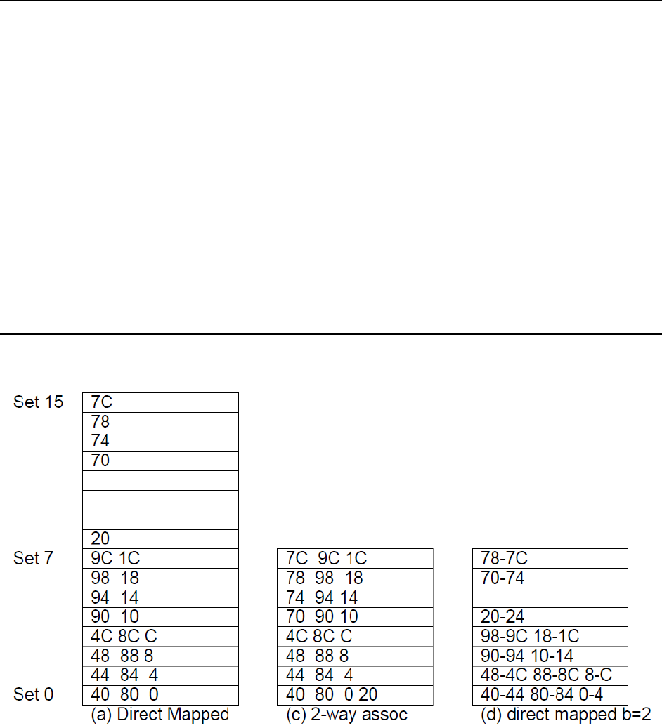
308
SOLUTIONS chapter 8 S. Harris and D.M. Harris, DDCA: ARM® Edition © 2015 Elsevier, Inc.
Exercise 8.7
(a) False.
Counterexample: A 2-word cache with block size of 1 word and access pattern:
0 4 8
This has a 50% miss rate with a direct-mapped cache, and a100% miss rate with a 2-way set
associative cache.
(b) True.
The 16KB cache is a superset of the 8KB cache. (Note: it’s possible that they have the same miss
rate.)
(c) Usually true.
Instruction memory accesses display great spatial locality, so a large block size reduces the miss
rate.
Exercise 8.9
The figure below shows where each address maps for each cache configuration.
(a) 80% miss rate. Addresses 70-7C and 20 use unique cache blocks and are not removed once
placed into the cache. Miss rate is 20/25 = 80%.
(b) 100% miss rate. A repeated sequence of length greater than the cache size produces no hits
for a fully-associative cache using LRU.

309
SOLUTIONS chapter 8 S. Harris and D.M. Harris, DDCA: ARM® Edition © 2015 Elsevier, Inc.
(c) 100% miss rate. The repeated sequence makes at least three accesses to each set during
each pass. Using LRU replacement, each value must be replaced each pass through.
(d) 40% miss rate. Data words from consecutive locations are stored in each cache block. The
larger block size is advantageous since accesses in the given sequence are made primarily to
consecutive word addresses. A block size of two cuts the number of block fetches in half since
two words are obtained per block fetch. The address of the second word in the block will
always hit in this type of scheme (e.g. address 44 of the 40-44 address pair). Thus, the second
consecutive word accesses always hit: 44, 4C, 74, 7C, 84, 8C, 94, 9C, 4, C, 14, 1C. Tracing block
accesses (see Figure 8.1) shows that three of the eight blocks (70-74, 78-7C, 20-24) also remain
in memory. Thus, the hit rate is: 15/25 = 60% and miss rate is 40%.
Exercise 8.11
(a) 128
(b) 100%
(c) ii
Exercise 8.13
(a)
(b) Each tag is 16 bits. There are 32Kwords / (2 words / block) = 16K blocks and each block
needs a tag: 16 × 16K = 218 = 256 Kbits of tags.
(c) Each cache block requires: 2 status bits, 16 bits of tag, and 64 data bits, thus each set is 2 ×
82 bits = 164 bits.
(d) See figure below. The design must use enough RAM chips to handle both the total capacity
and the number of bits that must be read on each cycle. For the data, the SRAM must provide a
capacity of 128 KB and must read 64 bits per cycle (one 32-bit word from each way). Thus the
design needs at least 128KB / (8KB/RAM) = 16 RAMs to hold the data and 64 bits / (4 pins/RAM)
= 16 RAMs to supply the number of bits. These are equal, so the design needs exactly 16 RAMs
for the data.

310
SOLUTIONS chapter 8 S. Harris and D.M. Harris, DDCA: ARM® Edition © 2015 Elsevier, Inc.
For the tags, the total capacity is 32 KB, from which 32 bits (two 16-bit tags) must be read each
cycle. Therefore, only 4 RAMs are necessary to meet the capacity, but 8 RAMs are needed to
supply 32 bits per cycle. Therefore, the design will need 8 RAMs, each of which is being used at
half capacity.
With 8K sets, the status bits require another 8K × 4-bit RAM. We use a 16K × 4-bit RAM, using
only half of the entries.
Bits 15:2 of the address select the word within a set and block. Bits 15-3 select the set. Bits
31:16 of the address are matched against the tags to find a hit in one (or none) of the two
blocks with each set.
Exercise 8.15
(a) FIFO: FIFO replacement approximates LRU replacement by discarding data that has been in
the cache longest (and is thus least likely to be used again). A FIFO cache can be stored as a
queue, so the cache need not keep track of the least recently used way in an N-way set-
associative cache. It simply loads a new cache block into the next way upon a new access. FIFO
replacement doesn’t work well when the least recently used data is not also the data fetched
longest ago.
Random: Random replacement requires less overhead (storage and hardware to update status
bits). However, a random replacement policy might randomly evict recently used data. In
practice random replacement works quite well.

311
SOLUTIONS chapter 8 S. Harris and D.M. Harris, DDCA: ARM® Edition © 2015 Elsevier, Inc.
(b) FIFO replacement would work well for an application that accesses a first set of data, then
the second set, then the first set again. It then accesses a third set of data and finally goes back
to access the second set of data. In this case, FIFO would replace the first set with the third set,
but LRU would replace the second set. The LRU replacement would require the cache to pull in
the second set of data twice.
Exercise 8.17
(a) AMAT = t
cache
+ MR
cache
t
MM
With a cycle time of 1/1 GHz = 1 ns,
AMAT = 1 ns + 0.15(200 ns) = 31 ns
(b) CPI = 31 + 4 = 35 cycles (for a load)
CPI = 31 + 3 = 34 cyles (for a store)
(c) Average CPI = (0.11 + 0.02)(3) + (0.52)(4) + (0.1)(34) + (0.25)(35) = 14.6
(d) Average CPI = 14.6 + 0.1(200) = 34.6
Exercise 8.19
From Figure 8.4, $1 million will buy about ($1 million / ($0.05/GB)) = 20 million GB of hard disk:
20 million GB ≈ 2
25
× 2
30
bytes = 2
55
bytes = 2
5
petabytes = 32 petabytes
$1 million will buy about ($1,000,000 / ($7/GB)) ≈143,000 GB of DRAM.
143,000 GB ≈ 2
7
× 2
10
× 2
30
= 2
47
bytes= 2
7
terabytes = 128 terabytes
Thus, the system would need 47 bits for the physical address and 55 bits for the virtual address.
Exercise 8.21
(a) 31 bits
(b) 2
50
/2
12
= 2
38
virtual pages
(c) 2 GB / 4 KB = 2
31
/2
12
= 2
19
physical pages
(d) virtual page number: 38 bits; physical page number = 19 bits
(e) 2
38
page table entries (one for each virtual page).
(f) Each entry uses 19 bits of physical page number and 2 bits of status information. Thus, 3
bytes are needed for each entry (rounding 21 bits up to thevnearest number of bytes).
(h)The total table size is 3 x 2
38
bytes.
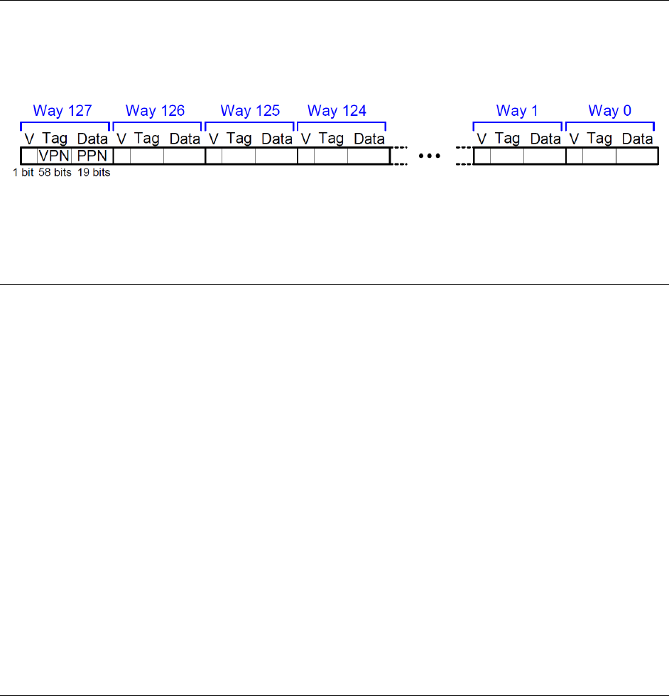
312
SOLUTIONS chapter 8 S. Harris and D.M. Harris, DDCA: ARM® Edition © 2015 Elsevier, Inc.
Exercise 8.23
(a) 1 valid bit + 19 data bits (PPN) + 38 tag bits (VPN) x 128 entries = 58 × 128 bits = 7424 bits
(b)
(c) 128 × 58-bit SRAM
Exercise 8.25
(a) Each entry in the page table has 2 status bits (V and D), and a physical page number (22-16 =
6 bits). The page table has 2
25 - 16
= 2
9
entries.
Thus, the total page table size is 2
9
× 8 bits = 4096 bits
(b) This would increase the virtual page number to 25 - 14 = 11 bits, and the physical page
number to 22 - 14 = 8 bits. This would increase the page table size to:
2
11
× 10 bits = 20480 bits
This increases the page table by 5 times, wasted valuable hardware to store the extra page
table bits.
(c) Yes, this is possible. In order for concurrent access to take place, the number of set + block
offset + byte offset bits must be less than the page offset bits.
(d) It is impossible to perform the tag comparison in the on-chip cache concurrently with the
page table access because the upper (most significant) bits of the physical address are unknown
until after the page table lookup (address translation) completes.
Exercise 8.27
(a) 2
32
bytes = 4 gigabytes
(b) The amount of the hard disk devoted to virtual memory determines how many applications
can run and how much virtual memory can be devoted to each application.
(c) The amount of physical memory affects how many physical pages can be accessed at once.
With a small main memory, if many applications run at once or a single application accesses

313
SOLUTIONS chapter 8 S. Harris and D.M. Harris, DDCA: ARM® Edition © 2015 Elsevier, Inc.
addresses from many different pages, thrashing can occur. This can make the applications
dreadfully slow.
Question 8.1
Caches are categorized based on the number of blocks (B) in a set. In a direct-mapped cache,
each set contains exactly one block, so the cache has S = B sets. Thus a particular main memory
address maps to a unique block in the cache. In an N-way set associative cache, each set
contains N blocks. The address still maps to a unique set, with S = B / N sets. But the data from
that address can go in any of the N blocks in the set. A fully associative cache has only S = 1 set.
Data can go in any of the B blocks in the set. Hence, a fully associative cache is another name
for a B-way set associative cache.
A direct mapped cache performs better than the other two when the data access pattern is to
sequential cache blocks in memory with a repeat length one greater than the number of blocks
in the cache.
An N-way set-associative cache performs better than the other two when N sequential block
accesses map to the same set in the set-associative and direct-mapped caches. The last set has
N+1 blocks that map to it. This access pattern then repeats.
In the direct-mapped cache, the accesses to the same set conflict, causing a 100% miss rate. But
in the set-associative cache all accesses (except the last one) don’t conflict. Because the
number of block accesses in the repeated pattern is one more than the number of blocks in the
cache, the fully associative cache also has a 100% miss rate.
A fully associative cache performs better than the other two when the direct- mapped and set-
associative accesses conflict and the fully associative accesses don’t. Thus, the repeated pattern
must access at most B blocks that map to conflicting sets in the direct and set-associative
caches.
Question 8.3
The advantages of using a virtual memory system are the illusion of a larger memory without
the expense of expanding the physical memory, easy relocation of programs and data, and
protection between concurrently running processes. The disadvantages are a more complex
314
SOLUTIONS chapter 8 S. Harris and D.M. Harris, DDCA: ARM® Edition © 2015 Elsevier, Inc.
memory system and the sacrifice of some physical and possibly virtual memory to store the
page table.
